ADAQ4224
PRE-RELEASE24-Bit, 2 MSPS, μModule Data Acquisition Solution
- Part Models
- 1
- 1ku List Price
- price unavailable
Part Details
- High Performance
- Throughput: 2 MSPS, no latency
- INL: ±1 ppm maximum from −40 °C to 105 °C
- Total system dynamic range: 128 dB typical
- SNR: 106.5 dB typical, THD: −122 dB typical
- Offset error drift: +4.1 μV/°C maximum
- Gain error drift: +1.50 ppm/°C maximum
- Ease of use features reduce system complexity
- Second-order, 270 kHz anti-aliasing filter
- High-Z PGIA gain options: 1/3, 5/9, 20/9, 20/3
- Flexible external reference voltage: 4.096 V or 5 V
- Differential Input Voltage ranges, ±REFIN/Gain: ±15 V, ±9 V, ±2.25 V, ±0.75 V
- Wide input common-mode voltage range: −8 V to +10 V
- Low input bias current: −30 pA typical
- High density solution reduces system footprint
- 14 mm × 9 mm, 0.8 mm pitch, 178-ball CSP BGA
- 4× footprint reduction vs. equivalent discrete solution
- On-board reference buffer with an internal VCM generation
- Total power dissipation: 446 mW typical at 2 MSPS
- Electrically isolated, 1.8 V I2C-compatible temperature sensor
- Flexi-SPI digital interface
- 1, 2, or 4 SDO lanes allows slower SCK
- Echo clock mode simplifies use of digital isolator
- Compatible with 1.2 V to 1.8 V logic
- PGIA gain control (A0, A1) interface
- Extended sample resolution to 30-bits
- Overrange and synchronization bits
The ADAQ4224 is a μModule® precision data acquisition (DAQ) signal chain solution that reduces the development cycle of a precision measurement system by transferring the signal chain design challenge of component selection, optimization, and layout from the designer to the device. With a guaranteed maximum ±1.0 ppm INL and no missing codes at 24 bits, the ADAQ4224 achieves unparalleled precision performance from −40°C to +105°C.
Using system-in-package (SIP) technology, the ADAQ4224 combines the common signal processing blocks required in a data acquisition solution in a small footprint, 14 mm × 9mm, 0.8 mm pitch, 178-ball CSP_BGA package.
The ADAQ4224 integrates the following:
- A low noise, high-bandwidth programmable gain instrumentation amplifier (PGIA).
- A second-order anti-aliasing filter.
- A low-noise, low-distortion, high-bandwidth ADC driver.
- A high precision 24-bit, 2 MSPS successive approximation register (SAR) ADC.
- An electrically isolated, I2C compatible temperature sensor with excellent accuracy of ±1°C maximum.
- A 1.8 V low dropout (LDO) regulator.
- Performance critical passives.
The ADAQ4224 incorporates the critical passive components with superior matching and drift characteristics using Analog Devices, Inc., iPassive® technology to minimize temperature dependent error sources and to offer optimized performance. Integrating the critical power supply and reference bypass capacitors reduce sensitivity to the system level board layout. Reducing the solution footprint enables addition of more functions within the system and hence the smaller form factor instruments without sacrificing performance.
The system integration solves many design challenges while the μModule still provides the flexibility of a configurable PGIA to allow gain or attenuation adjustments, as well as supports the acquisition of both single-ended and differential signals. The fast settling of the PGIA and ADC driver stage and no latency of the SAR ADC provide a unique solution for high channel count, multiplexed signal chain architectures and control loop applications.
The digital features include Flexi-SPI serial peripheral interface (SPI), which allow data access via multiple SPI modes as well as offset correction, gain adjustment, and averaging and reduce burden on the host processor. A wide data clocking window, multiple SDO lanes, and optional DDR data clocking reduce the serial clock frequency while operating at full speed of 2 MSPS and make it easier to isolate the DAQ solution, which reduces power dissipation and EMI. Echo clock mode and host clock mode of the ADAQ4224 relax the timing requirements and simplify the use of digital isolators.
The Flexi-SPI, PGIA gain control and I2C-compatible temperature sensor serial user interface is compatible with 1.2 V to 1.8 V, 2.5 V, 3 V, or 5 V logic, using a separate VIO supply. The ADAQ4224 operation is specified from −40°C to +105°C.
APPLICATIONS
- Automatic test equipment
- Machine automation
- Process controls
- Medical and industrial instrumentation
- Digital control loops
Documentation
Data Sheet 1
User Guide 1
ADI has always placed the highest emphasis on delivering products that meet the maximum levels of quality and reliability. We achieve this by incorporating quality and reliability checks in every scope of product and process design, and in the manufacturing process as well. "Zero defects" for shipped products is always our goal. View our quality and reliability program and certifications for more information.
| Part Model | Pin/Package Drawing | Documentation | CAD Symbols, Footprints, and 3D Models |
|---|---|---|---|
| ADAQ4224BBCZ | 178-ball CSP_BGA (14 mm x 9 mm x 1.706 mm) |
This is the most up-to-date revision of the Data Sheet.
Software Resources
Evaluation Software 3
Can't find the software or driver you need?
Hardware Ecosystem
| Parts | Product Life Cycle | Description |
|---|---|---|
| Charge Pumps 1 | ||
| LTC1983 | PRODUCTION | 100mA Regulated Charge-Pump Inverters in ThinSOT |
| Linear Regulators 3 | ||
| ADP7118 | RECOMMENDED FOR NEW DESIGNS | 20 V, 200 mA, Low Noise, CMOS LDO Linear Regulator |
| ADP7182 | RECOMMENDED FOR NEW DESIGNS | –28 V, −200 mA, Low Noise, Linear Regulator |
| ADP7183 | RECOMMENDED FOR NEW DESIGNS |
-300 mA, Ultralow Noise, High PSRR, Low Dropout Linear Regulator |
| Switching Regulators & Controllers 2 | ||
| LT3999 | PRODUCTION | Low Noise, 1A, 1MHz Push-Pull DC/DC Driver with Duty Cycle Control |
| LT3487 | PRODUCTION | Boost and Inverting Switching Regulator for CCD Bias |
| Voltage References 3 | ||
| ADR4540 | RECOMMENDED FOR NEW DESIGNS | Ultra-Low-Noise, High-Accuracy 4.096V Voltage Reference |
| ADR4550 | RECOMMENDED FOR NEW DESIGNS | Ultra-Low-Noise, High-Accuracy 5.0V Voltage Reference |
| LTC6655 | PRODUCTION | 0.25ppm Noise, Low Drift Precision References |
Tools & Simulations
LTspice 1
Precision ADC Driver Tool
The Precision ADC Driver Tool is a web application that simulates the performance of precision ADC and driver combinations. Potential issues with driver selection, kickback settling, and distortion are flagged, and design tradeoffs can be quickly evaluated. Simulations and calculations include system noise, distortion, and settling of the ADC input
Open ToolSignal Chain Designer - BETA
Signal Chain Designer is a web-based tool designed to create and simulate complex precision signal chains. See your circuit’s performance before you commit to your PCB: transfer function, noise, power consumption, input range, and DC error. Quickly experiment with different parts and architectures. Signal chains can be exported to LTspice for further analysis.
Open ToolIBIS Model 1
LTspice® is a powerful, fast and free simulation software, schematic capture and waveform viewer with enhancements and models for improving the simulation of analog circuits.
Evaluation Kits
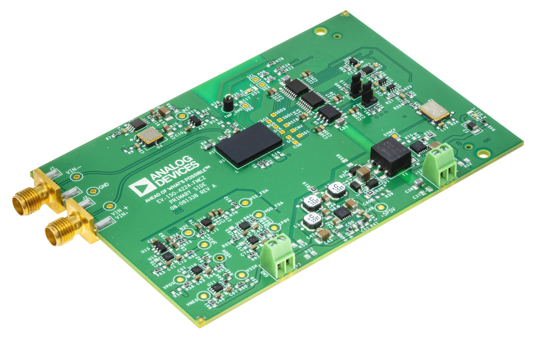
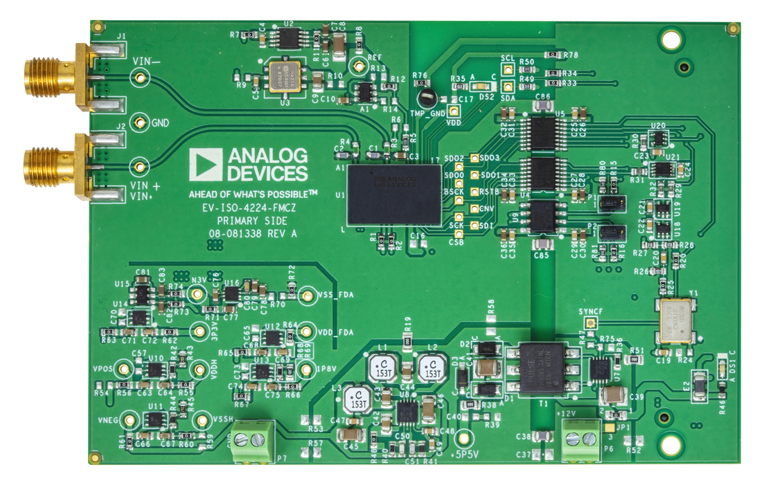
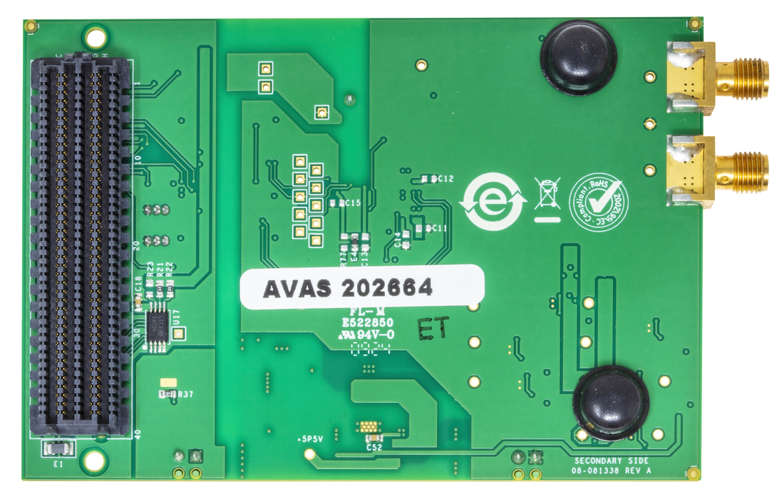
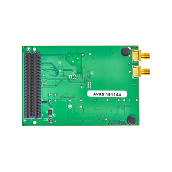
Isolated Digital and Power Reference Design for ADAQ4224
Resources
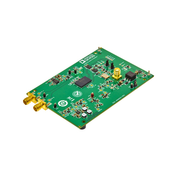
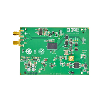
Evaluating the ADAQ4224 24-Bit, 2 MSPS, μModule Data-Acquisition Solution
Resources
Latest Discussions
No discussions on ADAQ4224 yet. Have something to say?
Start a Discussion on EngineerZone®