AD9166
RECOMMENDED FOR NEW DESIGNSDC to 9 GHz, Vector Signal Generator
- Part Models
- 2
- 1ku List Price
- Starting From $507.18
Part Details
- DC-coupled, 50 Ω matched output
- Up to 4.3 dBm output power, −9.5 dBm at 9 GHz
- DAC core update rate: 12.0 GSPS (guaranteed minimum) in 2× NRZ mode
- Wide analog bandwidth
- DC to 9.0 GHz in 2× NRZ mode (12.0 GSPS DAC update rate)
- 1.0 GHz to 8.0 GHz in mix mode (6.0 GSPS DAC update rate)
- DC to 4.5 GHz in NRZ mode (6.0 GSPS DAC update rate)
- Power dissipation of 4.88 W in 2× NRZ mode (10 GSPS DAC update rate)
- Bypassable datapath interpolation
- 2×, 3×, 4×, 6×, 8×, 12×, 16×, 24×
- Instantaneous (complex) signal bandwidth
- 2.25 GHz with device clock at 5 GHz (2× interpolation)
- 1.8 GHz with device clock at 6 GHz (3× interpolation)
- Fast frequency hopping
- Integrated biCMOS buffer amplifier
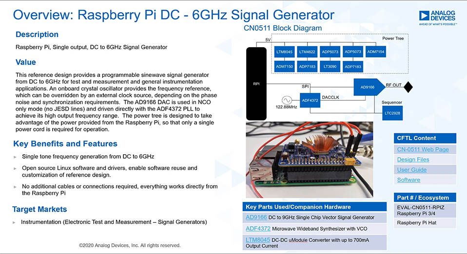
The AD91661 is a high performance, wideband, on-chip vector signal generator composed of a high speed JESD204B serializer/deserializer (SERDES) interface, a flexible 16-bit digital datapath, a inphase/quadrature (I/Q) digital-to-analog converter (DAC) core, and an integrated differential to single-ended output buffer amplifier, matched to a 50 Ω load up to 10 GHz.
The DAC core is based on a quad-switch architecture, which is configurable to increase the effective DAC core update rate of up to 12.8 GSPS from a 6.4 GHz DAC sampling clock, with an analog output bandwidth of true dc to 9.0 GHz, typically. The digital datapath includes multiple interpolation filter stages, a direct digital synthesizer (DDS) block with multiple numerically controlled oscillators (NCOs) supporting fast frequency hopping (FFH), and additional FIR85 and inverse sinc filter stages to allow flexible spectrum planning.
The differential to single-ended buffer eliminates the need for a wideband balun, and supports the full analog output bandwidth of the DAC core. DC coupling the output allows baseband waveform generation without the need for external bias tees or similar circuitry, which makes the AD9166 uniquely suited for the most demanding high speed ultrawideband RF transmit applications.
The various filter stages enable the AD9166 to be configured for lower data rates, while maintaining higher DAC clock rates to ease the filtering requirements and reduce the overall system size, weight, and power.
The data interface receiver consists of up to eight JESD204B SERDES lanes, each capable of carrying up to 12.5 Gbps. To enable maximum flexibility, the receiver is fully configurable according to the data rate, number of SERDES lanes, and lane mapping required by the JESD204B transmitter.
In 2× nonreturn-to-zero (NRZ) mode of operation (with FIR85 enabled), the AD9166 can reconstruct RF carriers from true dc to the edge of the third Nyquist zone, or an analog bandwidth of true dc up to 9 GHz.
In mix mode, the AD9166 can reconstruct RF carriers in the second and third Nyquist zones while consuming lower power and maintaining a performance comparable to 2× NRZ mode.
In baseband modes, such as return-to-zero (RZ) and 1× NRZ, the AD9166 is ideal to reconstruct RF carriers from true dc to the edge of the first Nyquist zone while consuming lower power compared to 2× NRZ mode.
The quadrature DDS block can be configured as a digital upconverter to upconvert I/Q data samples to the desired location across the spectrum, in all three Nyquist zones.
The DDS also consists of a bank of 32 numerically controlled oscillators (NCOs), each with its own 32-bit phase accumulator. When combined with a 100 MHz serial peripheral interface (SPI), the DDS allows a phase coherent FFH, with a phase settling time as low as 300 ns.
The AD9166 is configured using a common SPI interface that monitors the status of all registers. The AD9166 is offered in a 324-ball, 15 mm × 15 mm, 0.8 mm pitch BGA_ED package.
Product Highlights
- High dynamic range and signal reconstruction bandwidth supports RF signal synthesis of up to 9 GHz.
- Fully supports zero IF and other dc-coupled applications.
- Up to an eight-lane JESD204B SERDES interface, with various features to allow flexibility when interfacing to a JESD204B transmitter.
Applications
- Instrumentation: automated test equipment, electronic test and measurement, arbitrary waveform generators
- Electronic warfare: radars, jammers
- Broadband communications systems
- Local oscillator drivers
1 Protected by U.S. Patents 6,842,132 and 7,796,971.
Documentation
Data Sheet 1
User Guide 1
Technical Articles 2
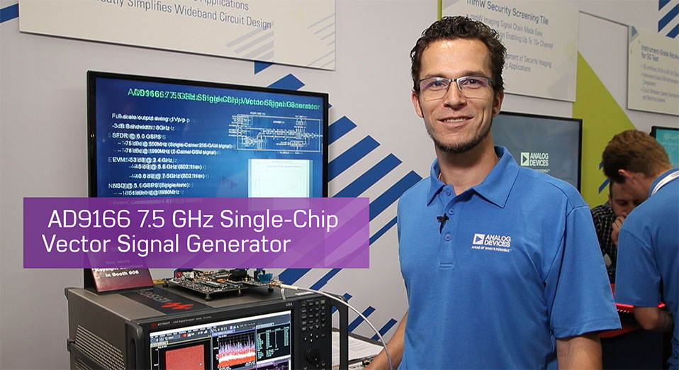
Video 2
Product Selection Guide 1
Analog Dialogue 1
ADI has always placed the highest emphasis on delivering products that meet the maximum levels of quality and reliability. We achieve this by incorporating quality and reliability checks in every scope of product and process design, and in the manufacturing process as well. "Zero defects" for shipped products is always our goal. View our quality and reliability program and certifications for more information.
| Part Model | Pin/Package Drawing | Documentation | CAD Symbols, Footprints, and 3D Models |
|---|---|---|---|
| AD9166BBPZ | 324-Ball BGA_ED (15mm x 15mm x 1.52mm) | ||
| AD9166BBPZRL | 324-Ball BGA_ED (15mm x 15mm x 1.52mm) |
This is the most up-to-date revision of the Data Sheet.
Software Resources
API Device Drivers 1
Device Application Programming Interface (API) C code drivers provided as reference code that allows the user to quickly configure the product using high-level function calls. The library acts as an abstraction layer between the application and the hardware. The API is developed in C99 to ensure agnostic processor and operating system integration. Customers can port this application layer code to their embedded systems by integrating their platform-specific code base to the API HAL layer.
To request this software package, go to the Software Request Form signed in with your MyAnalog account and under “Target Hardware” select “High Speed Data Converters” and choose the desired API product package. You will receive an email notification once the software is provided to you.
Evaluation Software 0
Can't find the software or driver you need?
Hardware Ecosystem
| Parts | Product Life Cycle | Description |
|---|---|---|
| Clock ICs 1 | ||
| HMC7044 | RECOMMENDED FOR NEW DESIGNS | High Performance, 3.2 GHz, 14-Output Jitter Attenuator with JESD204B and JESD204C Support |
| Fanout Buffers & Splitters 1 | ||
| HMC7043 | RECOMMENDED FOR NEW DESIGNS |
High Performance, 3.2 GHz, 14-Output Fanout Buffer with JESD204B/JESD204C |
| LDO Linear Regulators 5 | ||
| ADM7150 | RECOMMENDED FOR NEW DESIGNS | 800 mA, Ultra Low Noise/High PSRR LDO |
| ADM7154 | RECOMMENDED FOR NEW DESIGNS |
600 mA, Ultralow Noise, High PSRR, RF Linear Regulator |
| ADP1761 | RECOMMENDED FOR NEW DESIGNS | 1 A, Low VIN, Low Noise, CMOS Linear Regulator |
| LT3090 | RECOMMENDED FOR NEW DESIGNS | –36V, 600mA Negative Linear Regulator with Programmable Current Limit |
| ADP7183 | RECOMMENDED FOR NEW DESIGNS |
-300 mA, Ultralow Noise, High PSRR, Low Dropout Linear Regulator |
| Phase-Locked Loop (PLL) Synthesizers 1 | ||
| ADF4372 | RECOMMENDED FOR NEW DESIGNS | Microwave Wideband Synthesizer with Integrated VCO |
| Switching Regulators & Controllers 2 | ||
| ADP5073 | RECOMMENDED FOR NEW DESIGNS | 1.2 A, DC-to-DC Inverting Regulator |
| ADP5074 | RECOMMENDED FOR NEW DESIGNS | 2.4 A, DC-to-DC Inverting Regulator |
Tools & Simulations
S-Parameter 1
ADIsimDDS (Direct Digital Synthesis)
ADIsimDDS uses mathematical equations to model and illustrate the overall performance of the selected device. ADIsimDDS calculates the required FTW, given the reference clock frequency and desired output frequency. This tool also models an estimate of the overall spectral performance, and allows the user to explore the effects of external reconstruction filters.
Open ToolDAC Companion Transport Layer RTL Code Generator
These command line executable tool generates a Verilog module which implements the JESD204 transmitter transport layer. The user specifies in a configuration file one or more modes to be supported by the transport layer module. These modes are defined as a set of JESD204 parameter values: L, M, F, S, N', and CF. The transport layer converts JESD204 lane data output from a JESD204 link layer IP to a data bus with a fixed width, containing interleaved virtual converter samples. Both JESD204B and JESD204C link layers are supported.
Open ToolLTspice® is a powerful, fast and free simulation software, schematic capture and waveform viewer with enhancements and models for improving the simulation of analog circuits.
Evaluation Kits
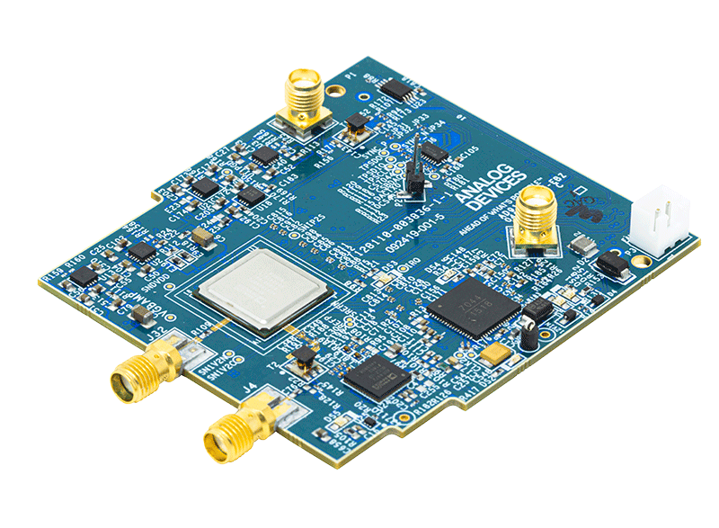
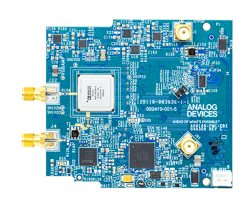

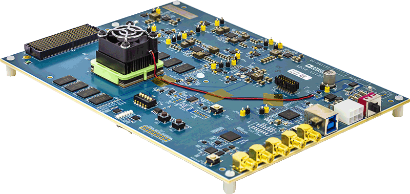
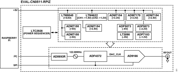
Evaluation Board for the AD9166 DC to 9 GHz Vector Signal Generator
Resources
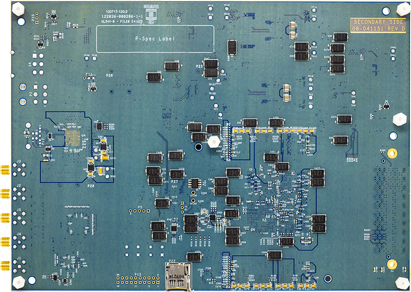
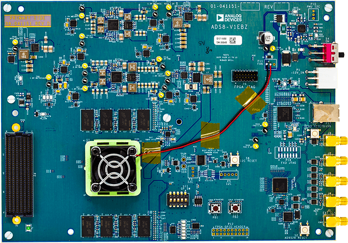
ADS8-V1 Evaluation Board
Resources
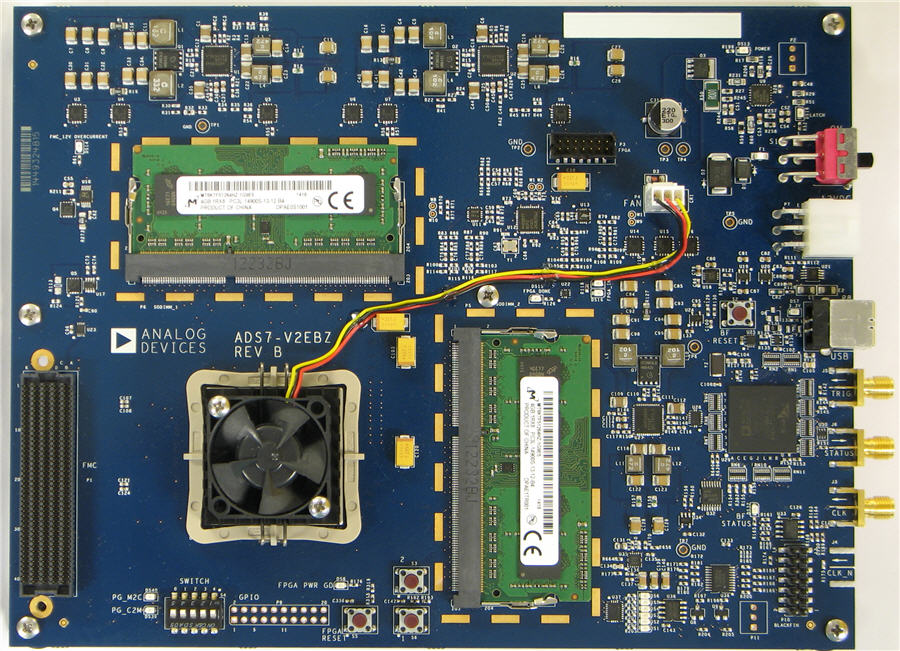
FPGA Based Data Capture Kit
Resources
Reference Designs

DC to 5.5 GHz Signal Generator with +/-0.5 dB Calibrated Output Power
Part Used
Resources
Design & Integration Tools
Latest Discussions
No discussions on AD9166 yet. Have something to say?
Start a Discussion on EngineerZone®