ADL8113
ADL8113
発売前10MHz to 12GHz Low Noise Amplifier with 10MHz to 14GHz Bypass Switches
Viewing:
製品の詳細
- Wideband amplifier with multiple bypass modes
- 4 pin-selectable operating modes
- Internal amplifier mode operating from 10MHz to 12GHz
- Internal bypass mode operating from 10MHz to 14GHz
- Two external bypass modes from 10MHz to 14GHz
- Integrated power-supply decoupling
- Reflective bypass switches
- In internal amplifier mode
- Small signal gain: 14.0dB typical from 200MHz to 6GHz
- OP1dB: 20.5dBm typical from 200MHz to 6GHz
- OIP3: 35.5dBm typical from 200MHz to 6GHz
- OIP2: 44.6dBm typical from 9GHz to 12GHz
- Noise figure: 3.8dB typical from 200MHz to 6GHz
- In internal bypass switch mode
- Insertion loss: 2.2dB typical from 200MHz to 6GHz
- Operating temperature range: −40°C to +85°C
- RoHS-compliant, 6mm × 6mm, 28-terminal LGA
The ADL8113 is a low noise amplifier (LNA) with bypass switches that provides broadband operation from 10MHz to 12GHz. The ADL8113 provides a low noise figure of 3.8dB and an output third-order intercept point (OIP3) of 35.5dBm from 200MHz to 6GHz. The ADL8113 provides a small signal gain of 14.0dB that is stable over frequency, temperature, power supply, and from device to device.
The integration of an amplifier and two SP4T reflective switches allows multiple paths through the device. The addition of switches also offers a high input third-order intercept (IIP3) path when large input signals are present. With the integration of power-supply decoupling capacitors, minimal external power-supply decoupling is required.
The ADL8113 is fully specified for operation across a temperature range of −40°C to +85°C. The ADL8113 is available in a 6mm × 6mm, 28-terminal land grid array (LGA) package.
APPLICATIONS
- Electronic test and measurement equipment
- Electronic warfare
- Wireless receivers
ドキュメント
データシート 1
ユーザ・ガイド 1
アプリケーション・ノート 1
これは最新改訂バージョンのデータシートです。
ツールおよびシミュレーション
Sパラメータ 1
評価用キット
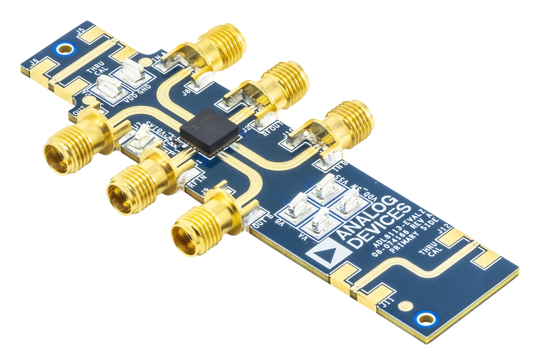
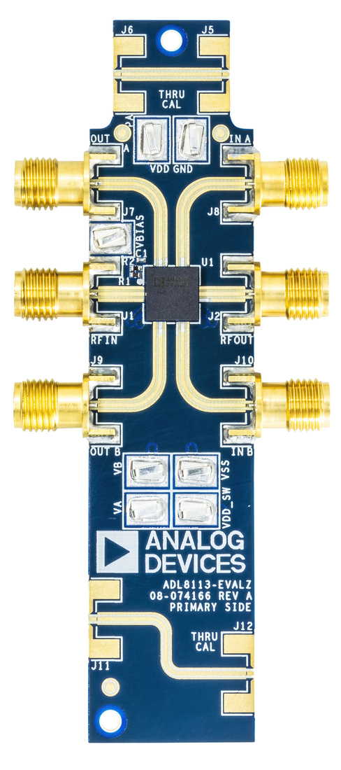
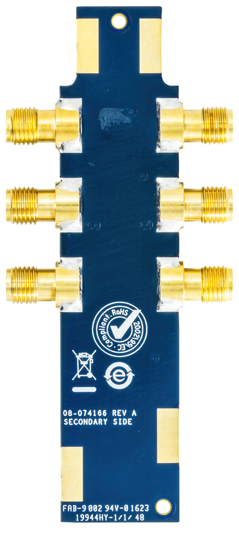
Evaluating the ADL8113 10MHz to 12GHz Low Noise Amplifier with 10MHz to 14GHz Bypass Switches
資料
最新のディスカッション
ADL8113に関するディスカッションはまだありません。意見を投稿しますか?
EngineerZone®でディスカッションを始める