ADA4352-2
発売前Dual-Channel, Precision, Programmable Gain Transimpedance Amplifier (PGTIA) with Integrated Gain Resistors
- 製品モデル
- 3
- 1Ku当たりの価格
- 価格は未定
製品の詳細
- Small, dual-channel, complete PGTIA and AFE solution
- Small size package: 16-lead LFCSP, 3 mm × 3 mm
- Integrated four internal gains per channel
- Range 0, internal RF = 315 Ω
- Range 1, internal RF = 3.5 kΩ
- Range 2, internal RF = 40.2 kΩ
- Range 3, internal RF = 450 kΩ
- Wide input current dynamic ranges from 100 picoamps to milliamps
- Excellent DC precision
- Low offset voltage: ±100 μV maximum, 25°C
- Low offset voltage drift: ±0.85 μV/°C maximum, −40°C to +125°C
- Low switch integrated switch impedance 19Ω maximum, −40°C to +125°C
- Excellent dynamic performance
- Range 0 settling time 1 µs
- Range 1 settling time 2 µs
- Range 2 settling time 5 µs
- Range 3 settling time 10 µs
- Kelvin-connected architecture eliminates gain error due to switch resistance over temperature.
- Single-supply operation: +2.7 V to +5.5 V (dual-supply operation: ±1.85 V to ±2.75 V)
- Wide gain bandwidth product: 8.5 MHz
- Wide operating temperature range: −40°C to +125°C
The ADA4352-2 is a compact, monolithic, dual-channel, precision, programmable gain transimpedance amplifier (PGTIA). The ADA4352-2 is a breakthrough solution for precisely measuring small currents over a wide dynamic range. The precision of the ADA4352-2 over a wide temperature range of −40°C to +125°C enables users to perform one calibration of the end equipment at room temperature, thereby saving test time and cost. The ADA4352-2 integrates four current-to-voltage gain selections per channel, and the gain is programmable using two logic pins per channel to provide a flexible, fully functional compact PGTIA solution. Additionally, with its robust output stage and low noise, the ADA4352-2 can directly drive 16-bit precision analog-to-digital converters (ADCs, such as AD4696), providing a complete analog front-end (AFE) to address the most challenging precision current measurement applications.
The ADA4352-2 is offered in a 3 mm × 3 mm LFCSP, reducing the printed circuit board (PCB) area by up to 10 times relative to a discrete design using standalone operational amplifiers (op amps) and switches.
Applications
- Precision current to voltage (I to V) conversion
- Programmable gain TIAs
- Photodetector interface and amplification
- Optical networking equipment
- Optical power measurement
- Instrumentation—spectroscopy and chromatography
- Precision data acquisition systems (DAQ)
ドキュメント
データシート 1
ユーザ・ガイド 1
ビデオ 1

| 製品モデル | ピン/パッケージ図 | 資料 | CADシンボル、フットプリント、および3Dモデル |
|---|---|---|---|
| ADA4352-2ACPZ | LFCSP:LEADFRM CHIP SCALE | ||
| ADA4352-2ACPZ-R7 | LFCSP:LEADFRM CHIP SCALE | ||
| ADA4352-2ACPZ-RL | LFCSP:LEADFRM CHIP SCALE |
これは最新改訂バージョンのデータシートです。
ハードウェア・エコシステム
| 製品モデル | 製品ライフサイクル | 詳細 |
|---|---|---|
| ADA4351-2 | 新規設計に推奨 | コンパクトなデュアル・チャンネル、高精度プログラマブル・ゲイン・トランスインピーダンス・アンプ(PGTIA) |
評価用キット
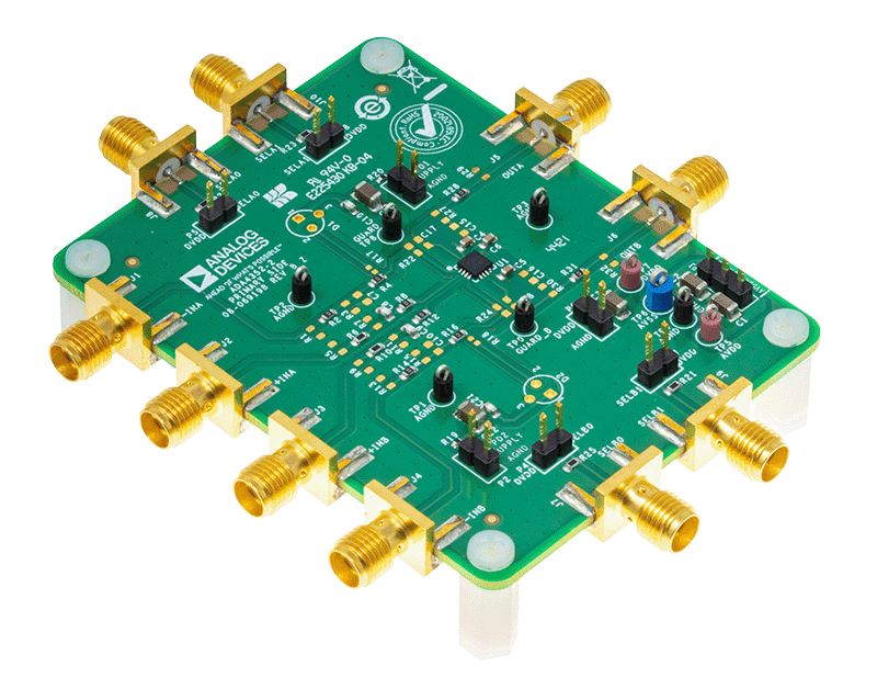
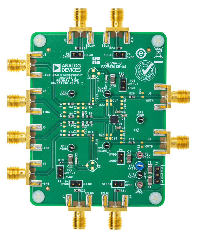
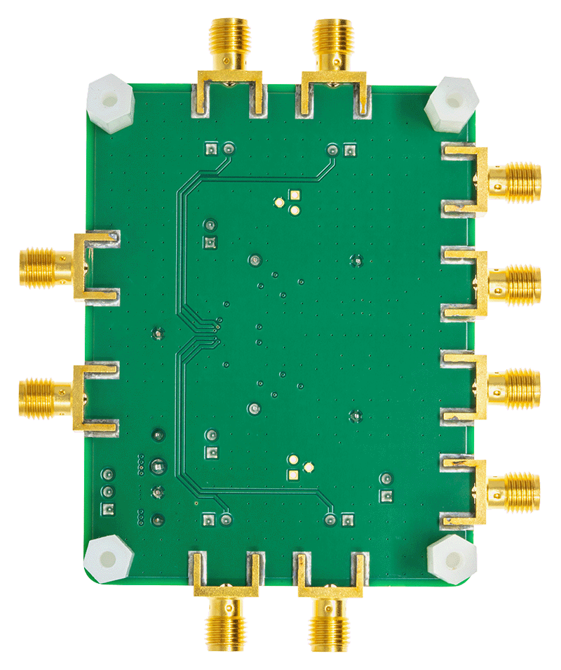
ADA4352-2評価用ボードのユーザ・ガイド
資料
最新のディスカッション
ADA4352-2に関するディスカッションはまだありません。意見を投稿しますか?
EngineerZone®でディスカッションを始める