ADAQ7767-1
RECOMMENDED FOR NEW DESIGNSFlexible Resistive Input, Anti-Alias, 24-Bit, 1 MSPS, μModule DAQ Solution
- Part Models
- 1
- 1ku List Price
- Starting From $13.65
Part Details
- Highly integrated data acquisition solution
- 3 pin-selectable gain options: 1 (IN1), 0.364 (IN2), or 0.143 (IN3)
- Maximum input range of ±28.672 V differential (IN3)
- Wide input common-mode range: −16 V to +12 V (IN3)
- Fourth-order AAF with maximum flatness and linear phase
- Anti-aliasing protection with 105 dB typical rejection (IN1)
- Excellent device-to-device phase matching and drift
- Combined precision ac and dc performance
- Total system dynamic range up to 124 dB
- -118 dB typical THD at ±28.672 V input range (IN3)
- 78.0 dB typical DC CMRR at ±28.672 V input range (IN3)
- ±3.8 ppm of FSR typical INL
- 3.1 ppm/°C max gain error drift
- ± 0.096 maximum device-to-device phase angle mismatch at 20 kHz
- Programmable output data rate, filter type, and latency
- Linear phase digital filter options:
- Wideband low ripple FIR filter (256 kSPS, 110 kHz maximum input bandwidth)
- Sinc5 Filter (1.024kSPS, 208.9 kHz maximum input bandwidth, 4 μs maximum group delay)
- Sinc3 Filter (50/60 Hz rejection)
- Linear phase digital filter options:
- Integrated LDO
- Built-in supply decoupling capacitors
- Configuration through pin strapping or SPI
- Digital interface optimized for isolated applications
- Suite of diagnostic check mechanisms
- Operating temperature range: −40°C to +105°C
- Packaging: 12 mm × 6 mm × 1.6 mm, 84-ball CSP_BGA with 0.8 mm ball pitch
- 8x footprint reduction vs. discrete solution
The ADAQ7767-1 is a 24-bit precision data acquisition (DAQ) μModule® system that encapsulates signal conditioning, conversion, and processing blocks into one system in package (SiP) design that enables rapid development of highly compact, high performance precision DAQ systems..
The ADAQ7767-1 consists of the following:
- A fourth order, low noise, linear phase anti-aliasing filter (AAF)
- A low noise, low distortion, high bandwidth, gain-selectable ADC driver plus an optional linearity boost buffer
- A high-performance medium bandwidth 24-bit sigma delta ADC with programmable digital filter
- A low noise, low dropout (LDO) linear regulator
- Reference buffers
- Critical passive components required for the signal chain
The ADAQ7767-1 supports a wide variety of input types, which include unipolar and bipolar single-ended, pseudo differential, and differential signals, with a maximum differential range of ±28.672 V and a common-mode voltage range of −16 V to +12 V using IN3. With the precision of Analog Devices iPASSIVES™ technology, the ADAQ7767-1 performs with excellent common-mode rejection ratio (CMRR). The three pairs of pin-selectable gain settings offer additional system dynamic range and improved signal chain noise performance with input signals of lower amplitude. In applications requiring high input impedance, the ADAQ7767-1 allows the customer to choose their preferred input amplifier.
A fourth-order low-pass analog filter combined with the user-programmable digital filter ensures that the signal chain is protected against the high frequency noise and out of band tones presented at the input node from aliasing back into the band of interest. The analog low pass filter is carefully designed to achieve high phase linearity and maximum in-band magnitude response flatness. Constructed with iPASSIVES technology, the resistor network used within the analog low-pass filter possess superior resistance matching in both absolute values and over temperature. As a result, the signal chain performance is maintained with minimum drift over temperature, and the ADAQ7767-1 has an excellent device-to-device phase matching performance.
A high-performance analog-to-digital (ADC) driver amplifier ensures the full settling of the ADC input at the maximum sampling rate. The driver circuit is designed to have minimum additive noise, error, and distortion while maintaining stability. The fully differential architecture helps maximizing the signal chain dynamic range.
The ADC inside the ADAQ7767-1 is a high performance, 24-bit precision, single-channel, Σ-Δ converter with excellent AC performance and DC precision, and a throughput rate of 1 MSPS from a 16.384 MHz MCLK. The device includes an optional linearity boost buffer that can further improve the signal chain linearity.
The ADAQ7767-1 is specified with an input reference voltage of 4.096 V, but the device can support reference voltages ranging from VDD_ADC down to 1 V.
The ADAQ7767-1 has two types of reference buffers: a precharge reference buffer to ease the reference input driving requirement, or a full reference buffer to provide a high impedance reference input. Both buffers are optional and can be turned off through register configuration.
The ADAQ7767-1 supports three clock input types: crystal, complementary metal-oxide semiconductor (CMOS), or low voltage differential signaling (LVDS).
Three types of digital low pass filters are available on the ADAQ7767-1. The wideband, low ripple, finite impulse response (FIR) filter has a filter profile similar to an ideal brick wall filter, making it a great fit for doing frequency analysis. The sinc5 filter has a low latency path with a smooth step response while maintaining a good level of aliasing rejection. This filter supports an output data rate up to 1.024 MSPS from a 16.384 MHz MCLK, making the sinc5 filter ideal for low latency data capturing and time domain analysis. The sinc3 filter supports a wide decimation ratio and can produce output data rates down to 50 SPS from a 16.384 MHz controller clock signal (MCLK). This combined with the simultaneous 50 Hz/60 Hz rejection post filter makes the sinc3 filter especially useful for precision DC measurement. All three digital filters on the ADAQ7767-1 are FIR filters with linear phase response. The bandwidth of the filters, which directly corresponds to the bandwidth of the DAQ signal chain, are fully programmable through register configuration.
The ADAQ7767-1 supports two device configuration methods. The user has the option to choose to configure the device via register write through its serial peripheral interface (SPI) or through a simple hardware pin strapping method to configure the device to operate under a number of predefined modes.
A single SPI supports both the register access and the sample data readback functions. The ADAQ7767-1 always acts as a SPI target. Multiple interface modes are supported with a minimum of three input and output channels required to communicate with the device.
The ADAQ7767-1 features a suite of internal diagnostic functions that can detect a broad range of errors during operation to help improve system reliability.
The ADAQ7767-1 supply connections can be simplified by using its internal low dropout (LDO) regulator. Note that, 0.1 μF decoupling capacitors are also integrated to further reduce the number of discrete components.
Each functional block of the device can be put into standby mode or power-down mode, enabling the ADAQ7767-1 to have a total power consumption less than 0.5 mW.
The ADAQ7767-1 has an operating temperature range of −40°C to +105°C and is available in a 12 mm x 6 mm, 84-ball CSP_BGA package with 0.8 mm ball pitch, making it suitable for multiple-channel applications. The footprint of the ADAQ7767-1 is eight times smaller compared to the footprint of the same solution using discrete components.
APPLICATIONS
- Universal input measurement platform
- Electrical Test and Measurement
- Sound and Vibration, Acoustic and Material Science, research and development
- Control and Hardware in Loop Verification
- Condition monitoring for predictive maintenance
- Audio Test
Protected by U.S. Patent 10,680,633 B1
Protected by U.S. Patent 10,979,062 B2
Documentation
Analog Dialogue 2
Webcast 1
ADI has always placed the highest emphasis on delivering products that meet the maximum levels of quality and reliability. We achieve this by incorporating quality and reliability checks in every scope of product and process design, and in the manufacturing process as well. "Zero defects" for shipped products is always our goal. View our quality and reliability program and certifications for more information.
| Part Model | Pin/Package Drawing | Documentation | CAD Symbols, Footprints, and 3D Models |
|---|---|---|---|
| ADAQ7767-1BBCZ | CHIP SCALE BGA |
Software Resources
Can't find the software or driver you need?
Request a Driver/SoftwareHardware Ecosystem
| Parts | Product Life Cycle | Description |
|---|---|---|
| Interface Transceivers & Isolators 1 | ||
| ADP1031 | RECOMMENDED FOR NEW DESIGNS | Three-Channel, Isolated Micropower Management Unit with Seven Digital Isolators |
| LDO Linear Regulators 3 | ||
| ADP7142 | RECOMMENDED FOR NEW DESIGNS | 40 V, 200 mA, Low Noise, CMOS LDO Linear Regulator |
| ADP7182 | RECOMMENDED FOR NEW DESIGNS | –28 V, −200 mA, Low Noise, Linear Regulator |
| ADP123 | PRODUCTION | 5.5 V Input, 300 mA, Low Quiescent Current, CMOS Linear Regulator, Adjustable Output Voltage |
| Operational Amplifiers 1 | ||
| LT3092 | PRODUCTION | 200mA 2-Terminal Programmable Current Source |
| Voltage References 1 | ||
| ADR4540 | RECOMMENDED FOR NEW DESIGNS | Ultra-Low-Noise, High-Accuracy 4.096V Voltage Reference |
Tools & Simulations
IBIS Model 1
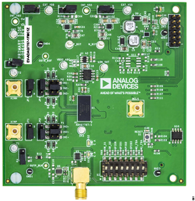
Evaluation Kits
Resources
Latest Discussions
No discussions on ADAQ7767-1 yet. Have something to say?
Start a Discussion on EngineerZone®