ADAQ23878
RECOMMENDED FOR NEW DESIGNS18-Bit, 15 MSPS, μModule Data Acquisition Solution
- Part Models
- 1
- 1ku List Price
- Starting From $42.32
Part Details
- Integrated fully differential ADC driver with signal scaling
- Wide input common-mode voltage range
- High common-mode rejection
- Single-ended to differential conversion
- Pin selectable input range with overrange
- Input ranges with 4.096 V REFBUF: ±10 V, ±5 V, ±4.096 V, ±2.5 V, and ±1.5 V
- Gain/attenuation options: 0.37, 0.73, 0.87, 1.38, and 2.25
- Critical passive components
- 0.005% precision matched resistor array for FDA
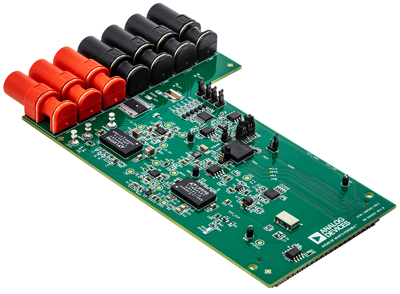
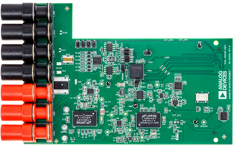
- 9 mm × 9 mm, 0.8 mm pitch, 100-ball CSP_BGA package
- 2.5× footprint reduction vs. discrete solution
- Low power, dynamic power scaling, power-down mode
- 143 mW typical at 15 MSPS
- Throughput: 15 MSPS, no pipeline delay
- INL error: ±3.1 ppm typical, ±6.2 ppm maximum
- (Gain = 0.73, gain = 0.87, gain = 1.38, gain = 2.25)
- SINAD: 90.4 dB typical at 20 kHz (gain = 0.73)
- THD: −117 dB at 1 kHz, −110 dB at 100 kHz (gain = 0.73)
- Gain error: ±0.005%FS typical
- Gain error drift: ±0.13 ppm/°C typical
- On-board reference buffer with VCMO generation
- Serial LVDS interface
- Wide operating temperature range: −40°C to +85°C
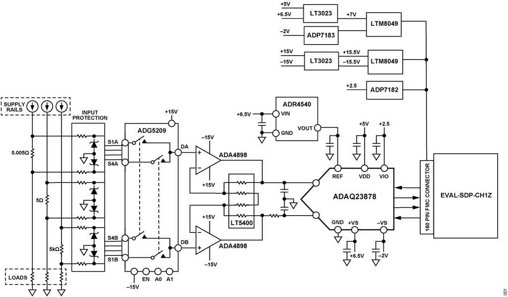
The ADAQ23878 is a precision, high speed, μModule® data acquisition solution that reduces the development cycle of a precision measurement systems by transferring the design burden of component selection, optimization, and layout from the designer to the device.
Using System-in-Package (SIP) technology, the ADAQ23878 reduces end system component count by combining multiple common signal processing and conditioning blocks in a single device, including a low noise, fully differential ADC driver (FDA), a stable reference buffer, and a high speed, 18-bit, 15 MSPS successive approximation register (SAR) ADC.
The ADAQ23878 also incorporates the critical passive components with superior matching and drift characteristics using Analog Devices, Inc., iPassive® technology to minimize temperature dependent error sources and to offer optimized performance. The fast settling of the ADC driver stage and no latency of the SAR ADC provide a unique solution for high channel count multiplexed signal chain architectures and control loop applications.
The small footprint, 9 mm × 9 mm BGA package enables smaller form factor instruments without sacrificing performance. The system integration solves many design challenges while the device still provides the flexibility of a configurable ADC driver feedback loop to allow gain or attenuation adjustments, as well as fully differential or single-ended to differential input. A single 5 V supply operation is possible while achieving optimum performance from the device.
The ADAQ23878 features a serial low voltage differential signaling (LVDS) digital interface with one-lane or two-lane output modes, allowing the user to optimize the interface data rate for each application. The specified operation of the ADAQ23878 is from −40°C to +85°C.
APPLICATIONS
- Automatic test equipment
- Data acquisition
- Hardware in the Loop (HiL)
- Power analyzers
- Non-destructive test (acoustic emissions)
- Mass spectrometry
- Travelling wave fault location
- Medical imaging and instruments
Documentation
Data Sheet 1
User Guide 2
Video 5


Device Drivers 2
Analog Dialogue 2
Webcast 3
ADI has always placed the highest emphasis on delivering products that meet the maximum levels of quality and reliability. We achieve this by incorporating quality and reliability checks in every scope of product and process design, and in the manufacturing process as well. "Zero defects" for shipped products is always our goal. View our quality and reliability program and certifications for more information.
| Part Model | Pin/Package Drawing | Documentation | CAD Symbols, Footprints, and 3D Models |
|---|---|---|---|
| ADAQ23878BBCZ | 100-Ball CSP-BGA (9mm x 9mm x 2.268mm) |
This is the most up-to-date revision of the Data Sheet.
Software Resources
Code Examples 1
Evaluation Software 0
Can't find the software or driver you need?
Tools & Simulations
LTspice 3
- ADAQ23878 Demo Circuit – 18-Bit, 15 MSPS, μModule Data Acquisition Solution
- Density Optimized LTspice Signal Chain Simulation
- ADAQ23878 - Integrated/Special Purpose A/D Converters
Models for the following parts are available in LTspice:
- ADAQ23878
IBIS Model 1
LTPowerPlanner 1
Signal Chain Designer - BETA
Signal Chain Designer is a web-based tool designed to create and simulate complex precision signal chains. See your circuit’s performance before you commit to your PCB: transfer function, noise, power consumption, input range, and DC error. Quickly experiment with different parts and architectures. Signal chains can be exported to LTspice for further analysis.
Open ToolLTspice® is a powerful, fast and free simulation software, schematic capture and waveform viewer with enhancements and models for improving the simulation of analog circuits.
Evaluation Kits
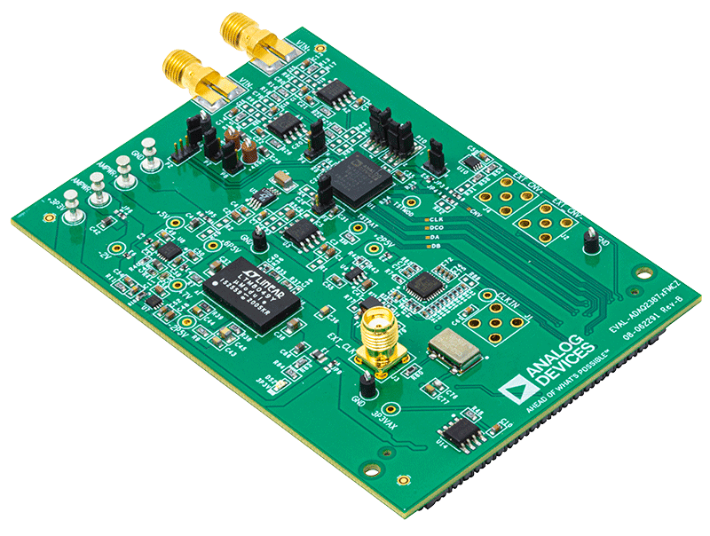
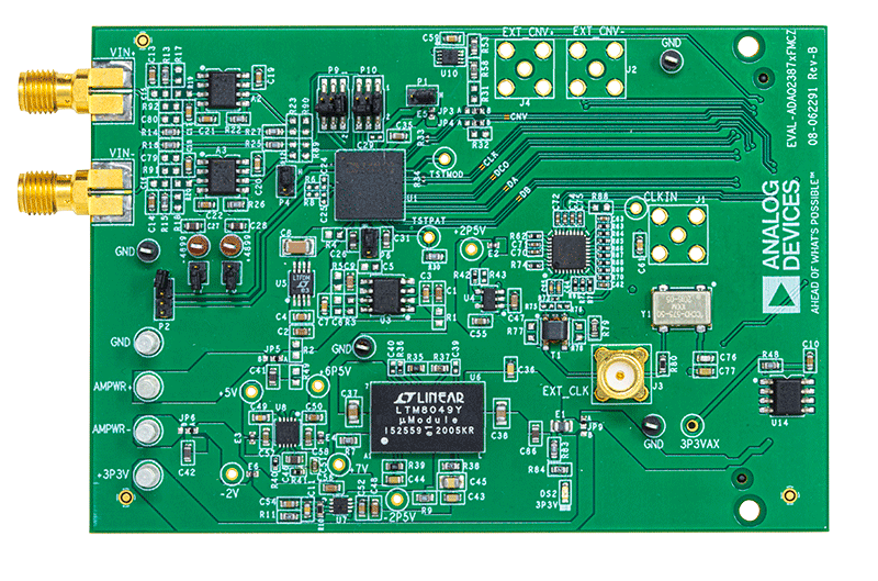
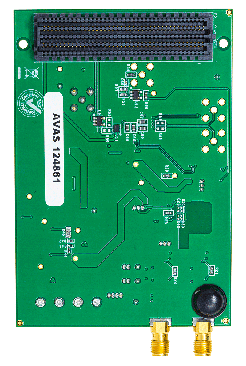
Evaluating the ADAQ23878 18-Bit, 15 MSPS, μModule Data Acquisition Solution
Resources
Reference Designs

High Precision, Wide Bandwidth Current Measurement Signal Chain
Part Used
Design & Integration Tools
Latest Discussions
No discussions on ADAQ23878 yet. Have something to say?
Start a Discussion on EngineerZone®