AD9163
RECOMMENDED FOR NEW DESIGNS16-Bit, 12 GSPS, RF DAC and Digital Upconverter
- Part Models
- 2
- 1ku List Price
- Starting From $114.28
Part Details
- DAC update rate up to 12 GSPS (minimum)
- Direct RF synthesis at 6 GSPS (minimum)
- DC to 3 GHz in nonreturn-to-zero (NRZ) mode
- DC to 6 GHz in 2× NRZ mode
- 1.5 GHz to 7.5 GHz in Mix-Mode
- Selectable interpolation
- 6×, 8×, 12×, 16×, 24×
- Excellent dynamic performance
The AD91631 is a high performance, 16-bit digital-to-analog converter (DAC) that supports data rates to 6 GSPS. The DAC core is based on a quad-switch architecture coupled with a 2× interpolator filter that enables an effective DAC update rate of up to 12 GSPS in some modes. The high dynamic range and bandwidth makes this DAC ideally suited for the most demanding high speed radio frequency (RF) DAC applications.
Superior RF performance and deep interpolation rates enable use of the AD9163 in many wireless infrastructure applications, including MC-GSM, W-CDMA, LTE, and LTE-A.
The wide bandwidth of up to 1 GHz and the complex NCO and digital upconverter enable dual band and triple band direct RF synthesis of wireless infrastructure signals, eliminating costly analog upconverters.
Wide analog bandwidth capability combines with high dynamic range to support DOCSIS 3.1 cable infrastructure compliance from the minimum of one carrier up to 1 GHz of signal bandwidth, making it ideal for cable multiple dwelling unit (MDU) applications. A 2× interpolator filter (FIR85) enables the AD9163 to be configured for lower data rates and converter clocking to reduce the overall system power and ease the filtering requirements. In Mix-Mode™ operation, the AD9163 can reconstruct RF carriers in the second and third Nyquist zones up to 7.5 GHz while still maintaining exceptional dynamic range. The output current can be programmed from 8 mA to 38.76 mA. The AD9163 data interface consists of up to eight JESD204B serializer/deserializer (SERDES) lanes that are programmable in terms of lane speed and number of lanes to enable application flexibility.
A serial peripheral interface (SPI) configures the AD9163 and monitors the status of all the registers. The AD9163 is offered in a 169-ball, 11 mm × 11 mm, 0.8 mm pitch CSP_BGA package.
Product Highlights
- High dynamic range and signal reconstruction bandwidth supports RF signal synthesis of up to 7.5 GHz.
- Up to eight lanes JESD204B SERDES interface, flexible in terms of number of lanes and lane speed.
- Bandwidth and dynamic range to meet multiband wireless communications standards with margin.
Applications
- Broadband communications systems
- DOCSIS 3.1 cable modem termination system (CMTS)/ video on demand (VOD)/edge quadrature amplitude modulation (EQAM)
- Wireless communications infrastructure
- MC-GSM, W-CDMA, LTE, LTE-A, point to point
Documentation
Data Sheet 1
User Guide 1
Technical Articles 1
Device Drivers 1
FPGA Interoperability Reports 1
Analog Dialogue 1
Webcast 2
ADI has always placed the highest emphasis on delivering products that meet the maximum levels of quality and reliability. We achieve this by incorporating quality and reliability checks in every scope of product and process design, and in the manufacturing process as well. "Zero defects" for shipped products is always our goal. View our quality and reliability program and certifications for more information.
| Part Model | Pin/Package Drawing | Documentation | CAD Symbols, Footprints, and 3D Models |
|---|---|---|---|
| AD9163BBCZ | 169-Ball CSPBGA (11mm x 11mm x 0.95mm) | ||
| AD9163BBCZRL | 169-Ball CSPBGA (11mm x 11mm x 0.95mm) |
| Part Models | Product Lifecycle | PCN |
|---|---|---|
|
Jan 30, 2020 - 20_0020 AD9161/AD9162/AD9163/AD9164 Die Revision |
||
| AD9163BBCZ | PRODUCTION | |
| AD9163BBCZRL | PRODUCTION | |
This is the most up-to-date revision of the Data Sheet.
Software Resources
Device Drivers 1
AD916x API
API library for the AD916x family of 11-Bit/16-Bit, 12 GSPS, RF Digital-to-Analog Converters
View DetailsEvaluation Software 1
JESD204x Frame Mapping Table Generator
The JESD204x Frame Mapping Table Generator tool consists of two Windows executables that will allow the user to input any valid combination of JESD204x parameters (L, M, F, S, NP) in order to output a .csv file that illustrates the frame mapping of the JESD204x mode in table format. There is an executable that allows the user to input a single JESD204x mode and another, that allows the user to input the parameters for multiple JESD204x modes in a specified .csv format in order to output a .csv file that illustrates the frame mapping of each of the JESD204x modes that were input into separate tables.
Can't find the software or driver you need?
Hardware Ecosystem
| Parts | Product Life Cycle | Description |
|---|---|---|
| Clock ICs 2 | ||
| HMC7044 | RECOMMENDED FOR NEW DESIGNS | High Performance, 3.2 GHz, 14-Output Jitter Attenuator with JESD204B and JESD204C Support |
| LTC6952 | LAST TIME BUY | Ultralow Jitter, 4.5GHz PLL with 11 Outputs and JESD204B / JESD204C Support |
| Fanout Buffers & Splitters 1 | ||
| LTC6955 | LAST TIME BUY | Ultralow Jitter, 7.5GHz, 11 Output Fanout Buffer Family |
| Phase-Locked Loop (PLL) Synthesizers 1 | ||
| ADF4377 | RECOMMENDED FOR NEW DESIGNS | Microwave Wideband Synthesizer with Integrated VCO |
Tools & Simulations
Using MATLAB with ADS7 and AD916x Eval Boards
The AD916x evaluation boards can be used and controlled by a MATLAB simulation. This enables users to verify simulation results by running on actual hardware.
Open ToolADIsimRF
ADIsimRF is an easy-to-use RF signal chain calculator. Cascaded gain, noise, distortion and power consumption can be calculated, plotted and exported for signal chains with up to 50 stages. ADIsimRF also includes an extensive data base of device models for ADI’s RF and mixed signal components.
Open ToolDAC Companion Transport Layer RTL Code Generator
These command line executable tool generates a Verilog module which implements the JESD204 transmitter transport layer. The user specifies in a configuration file one or more modes to be supported by the transport layer module. These modes are defined as a set of JESD204 parameter values: L, M, F, S, N', and CF. The transport layer converts JESD204 lane data output from a JESD204 link layer IP to a data bus with a fixed width, containing interleaved virtual converter samples. Both JESD204B and JESD204C link layers are supported.
Open ToolIBIS Model 1
Evaluation Kits
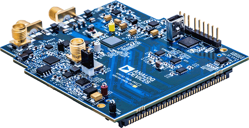
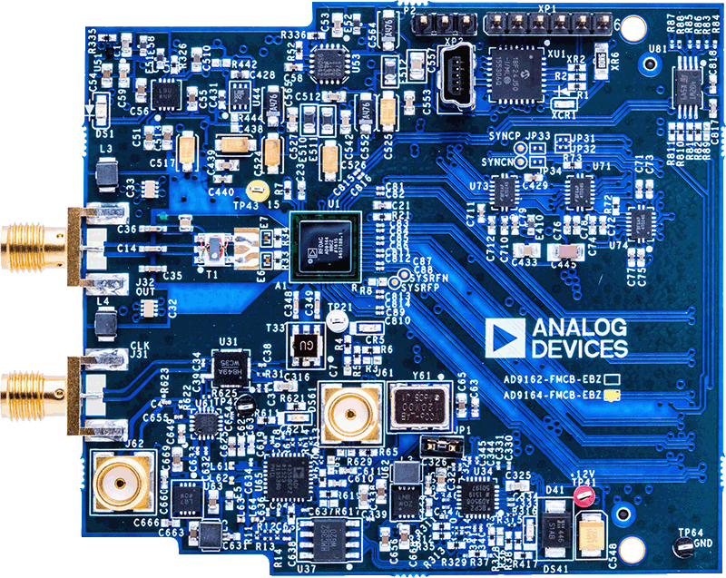
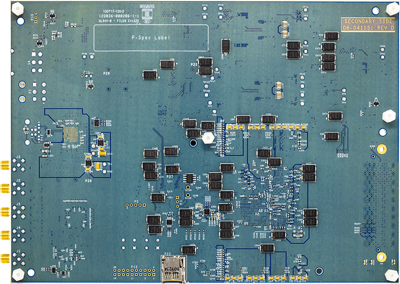
AD9161/AD9162/AD9163/AD9164 Evaluation Board
Resources
Software
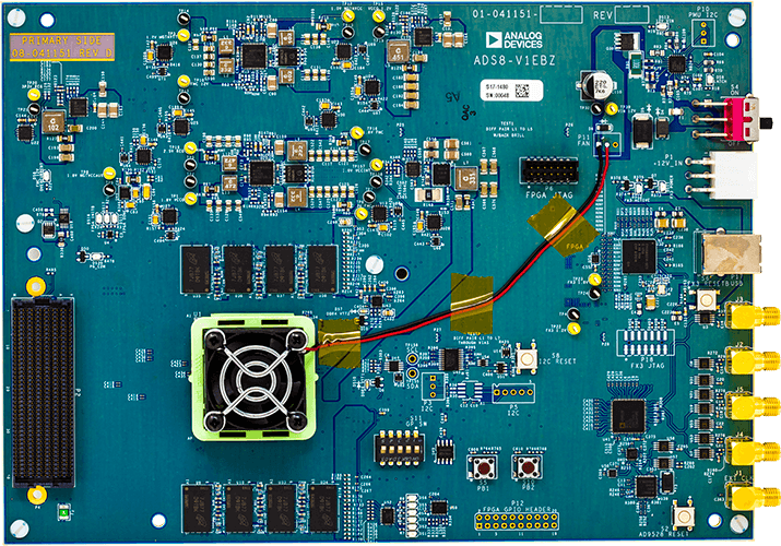
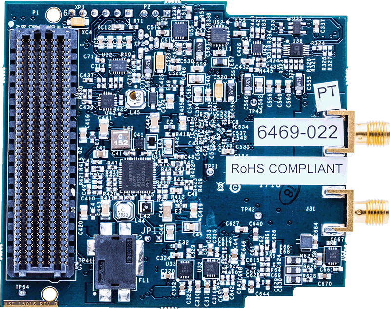
ADS8-V1 Evaluation Board
Resources
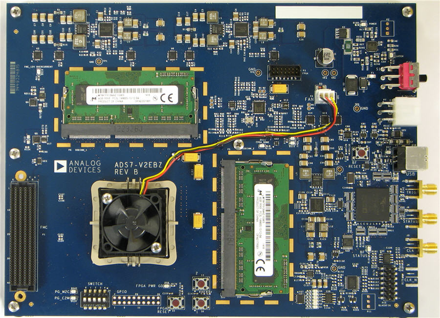
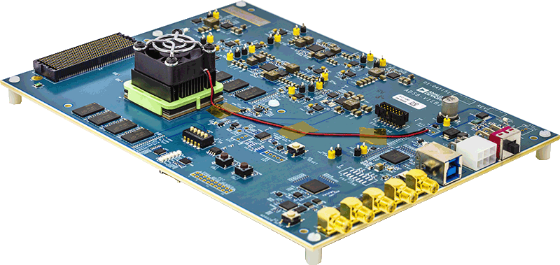
FPGA Based Data Capture Kit
Resources
Latest Discussions
No discussions on AD9163 yet. Have something to say?
Start a Discussion on EngineerZone®