AD9148
RECOMMENDED FOR NEW DESIGNSQuad 16-Bit,1GSPS DAC TxDAC+ Digital-to-Analog Converter
- Part Models
- 4
- 1ku List Price
- Starting From $72.93
Part Details
- Single carrier WCDMA ACLR = 80 dBc @ 150 MHz IF
- Channel to Channel Isolation > 90dB
- Analog output
- Adjustable 8.7 mA to 31.7 mA
- RL = 25 Ω to 50 Ω
- Novel 2×, 4× and 8x interpolator eases data interface
- On-chip fine complex NCO allows carrier placement anywhere in DAC bandwidth
- High performance, low noise PLL clock multiplier
- Multiple chip synchronization interface
- Programmable digital inverse sinc filter
- Auxiliary DACs allow for offset control
- Gain DACs allow for I and Q gain matching
- Programmable I and Q phase compensation
- Digital gain control
- Flexible LVDS digital I/F supports 32- or 16-bit bus width
- 196-ball CSP_BGA, 12 mm × 12 mm
The AD9148 is a quad, 16-bit, high dynamic range, digital-to-analog converter (DAC) that provides a sample rate of 1000 MSPS. These devices include features optimized for direct conversion transmit applications, including gain, phase, and offset compensation. The DAC outputs are optimized to interface seamlessly with analog quadrature modulators such as the ADL5371 / ADL5372 / ADL5373 / ADL5374 /ADL5375. A serial peripheral interface (SPI) is provided for programming of the internal device parameters. Full-scale output current can be programmed over a range of 10 mA to 30 mA. The devices operate from 1.8 V and 3.3 V supplies for a total power consumption of 3 W at the maximum sample rate. They are enclosed in 196-ball chip scale package ball grid array with the option of an attached heat spreader.
PRODUCT HIGHLIGHTS
- Low noise and intermodulation distortion (IMD) enable high quality synthesis of wideband signals from baseband to high intermediate frequencies.
- A proprietary DAC output switching technique enhances dynamic performance.
- The current outputs are easily configured for various single-ended or differential circuit topologies.
- The LVDS data input interface includes FIFO to ease input timing.
APPLICATIONS
- Wireless infrastructure
- LTE, TD-SCDMA, WiMAX, W-CDMA, CDMA2000, GSM
- MIMO/transmit diversity
- Digital high or low IF synthesis
Documentation
Data Sheet 1
User Guide 1
Application Note 2
Evaluation Design File 5
Solutions Bulletin & Brochure 1
ADI has always placed the highest emphasis on delivering products that meet the maximum levels of quality and reliability. We achieve this by incorporating quality and reliability checks in every scope of product and process design, and in the manufacturing process as well. "Zero defects" for shipped products is always our goal. View our quality and reliability program and certifications for more information.
| Part Model | Pin/Package Drawing | Documentation | CAD Symbols, Footprints, and 3D Models |
|---|---|---|---|
| AD9148BBCZ | 196-Ball CSPBGA (12mm x 12mm x 1.3mm) | ||
| AD9148BBCZRL | 196-Ball CSPBGA (12mm x 12mm x 1.3mm) | ||
| AD9148BBPZ | 196-Ball BGA (12mm x 12mm x 1.32mm w/ EP) | ||
| AD9148BBPZRL | 196-Ball BGA (12mm x 12mm x 1.32mm w/ EP) |
| Part Models | Product Lifecycle | PCN |
|---|---|---|
|
Feb 11, 2015 - 14_0254 Bump and Assembly Transfer of Select 10x10 and 12x12 Flip Chip Products |
||
| AD9148BBCZ | PRODUCTION | |
| AD9148BBCZRL | PRODUCTION | |
| AD9148BBPZ | PRODUCTION | |
| AD9148BBPZRL | PRODUCTION | |
|
Nov 2, 2011 - 11_0269 AD9148 Datasheet and Die Revision |
||
| AD9148BBCZ | PRODUCTION | |
| AD9148BBCZRL | PRODUCTION | |
| AD9148BBPZ | PRODUCTION | |
| AD9148BBPZRL | PRODUCTION | |
This is the most up-to-date revision of the Data Sheet.
Software Resources
Can't find the software or driver you need?
Request a Driver/SoftwareHardware Ecosystem
| Parts | Product Life Cycle | Description |
|---|---|---|
| Clock ICs 7 | ||
| AD9510 | RECOMMENDED FOR NEW DESIGNS | 1.2 GHz Clock Distribution IC, PLL Core, Dividers, Delay Adjust, Eight Outputs |
| AD9511 | RECOMMENDED FOR NEW DESIGNS | 1.2 GHz Clock Distribution IC, PLL Core, Dividers, Delay Adjust, Five Outputs |
| AD9512 | RECOMMENDED FOR NEW DESIGNS | 1.2 GHz Clock Distribution IC, Two 1.6 GHz Inputs, Dividers, Delay Adjust, Five Outputs |
| AD9513 | RECOMMENDED FOR NEW DESIGNS | 800 MHz Clock Distribution IC, Dividers, Delay Adjust, Three Outputs |
| AD9514 | RECOMMENDED FOR NEW DESIGNS | 1.6 GHz Clock Distribution IC, Dividers, Delay Adjust, Three Outputs |
| AD9515 | RECOMMENDED FOR NEW DESIGNS | 1.6 GHz Clock Distribution IC, Dividers, Delay Adjust, Two Outputs |
| AD9516-1 | RECOMMENDED FOR NEW DESIGNS | 14-Output Clock Generator with Integrated 2.5 GHz VCO |
| Modulators & Demodulators 15 | ||
| AD8345 | PRODUCTION | 140 MHz to 1000 MHz Quadrature Modulator |
| AD8346 | PRODUCTION | 2.5 GHz Direct Conversion Quadrature Modulator |
| AD8349 | PRODUCTION | 700 MHz TO 2.7 GHz Direct Up-Conversion Quadrature Modulator |
| ADL5370 | PRODUCTION | 300 MHz TO 1000 MHz Quadrature Modulator |
| ADL5371 | RECOMMENDED FOR NEW DESIGNS | 500 MHz TO 1500 MHz Quadrature Modulator |
| ADL5372 | PRODUCTION | 1500 MHz TO 2500 MHz Quadrature Modulator |
| ADL5373 | PRODUCTION | 2300 MHz TO 3000 MHz Quadrature Modulator |
| ADL5374 | Obsolete | 3000 MHz TO 4000 MHz Quadrature Modulator |
| ADL5375 | PRODUCTION | 400 MHz TO 6 GHz Broadband Quadrature Modulator |
| ADL5385 | RECOMMENDED FOR NEW DESIGNS | 30 MHz TO 2200 MHz Quadrature Modulator |
| ADL5386 | Obsolete | 50 MHz to 2200 MHz Quadrature Modulator with Integrated Detector and VVA |
| ADRF6701 | Obsolete | 400 MHz to 1250 MHz Quadrature Modulator with 750 MHz to 1150 MHz Fractional-N PLL and Integrated VCO |
| ADRF6702 | Obsolete | 1200 MHz to 2400 MHz Quadrature Modulator with 1550 MHz to 2150 MHz Fractional-N PLL & Integrated VCO |
| ADRF6703 | Obsolete | 1550 MHz to 2650 MHz Quadrature Modulator with 2100 MHz to 2600 MHz Fractional-N PLL & Integrated VCO |
| ADRF6704 | Obsolete | 2050 MHz to 3000 MHz Quadrature Modulator with 2500 MHz to 2900 MHz Fractional-N PLL & Integrated VCO |
| Operational Amplifiers 2 | ||
| AD8022 | PRODUCTION | Dual High Speed, Low Noise Op Amp |
| ADA4841-2 | PRODUCTION | Low Power, Low Noise and Distortion, Rail-to-Rail Output Amplifier |
Tools & Simulations
IBIS Model 1
Evaluation Kits

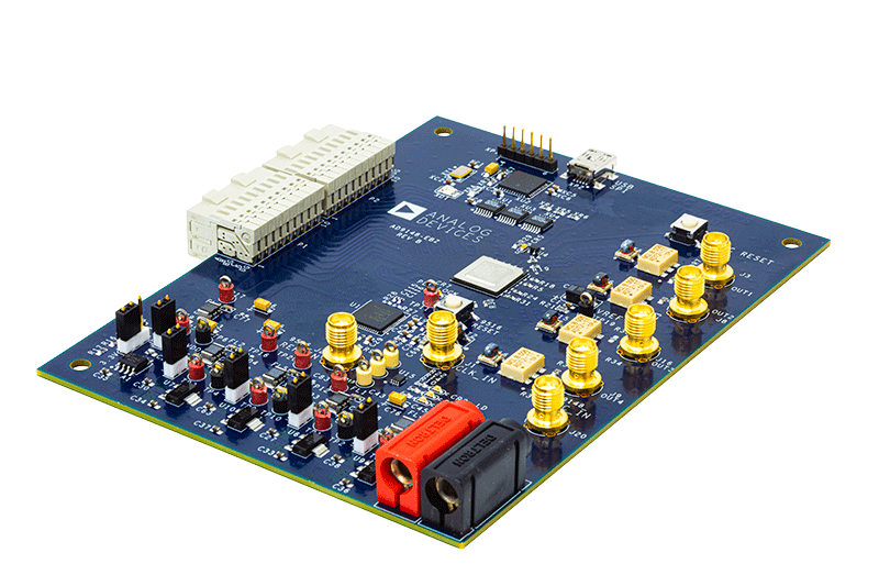
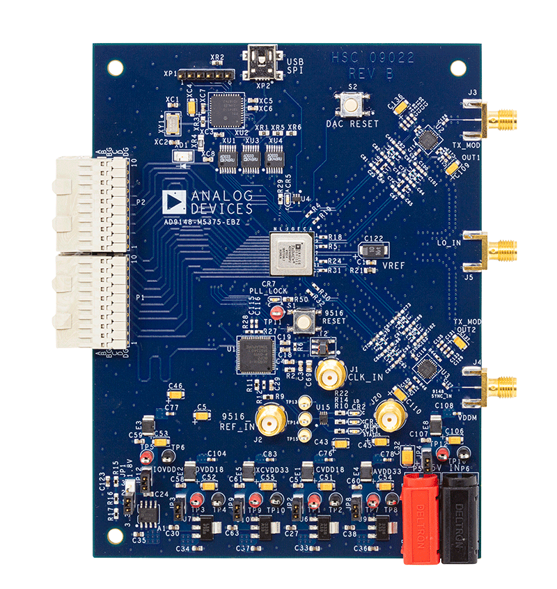
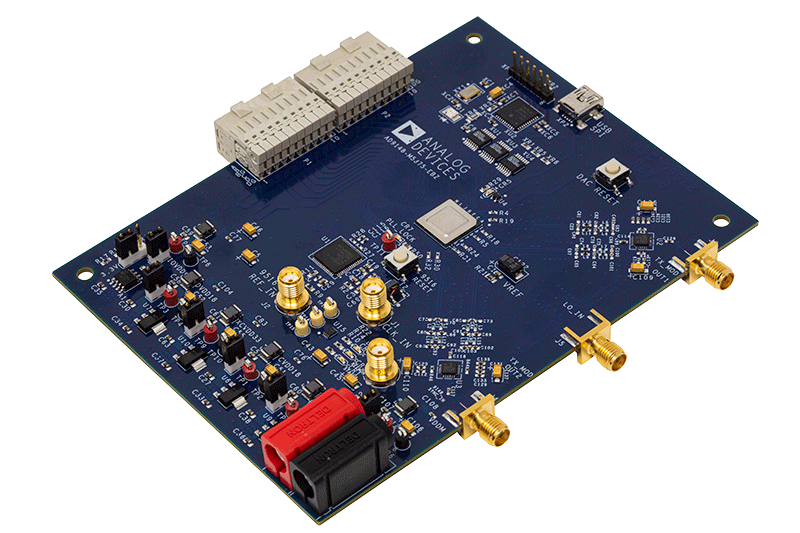

AD9148 Evaluation Board
Resources
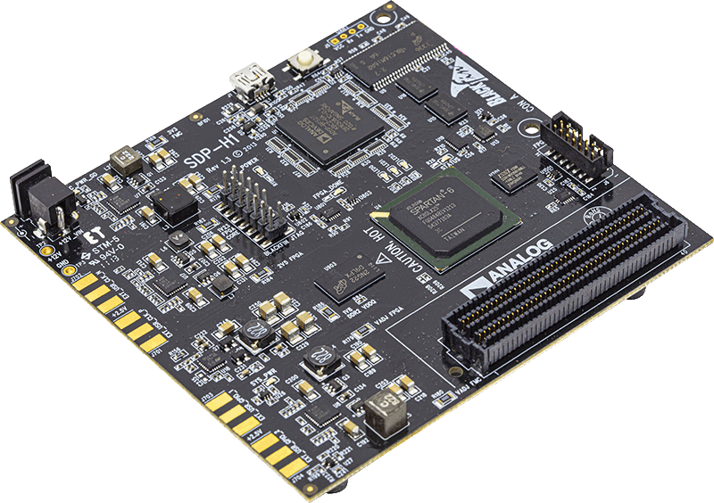

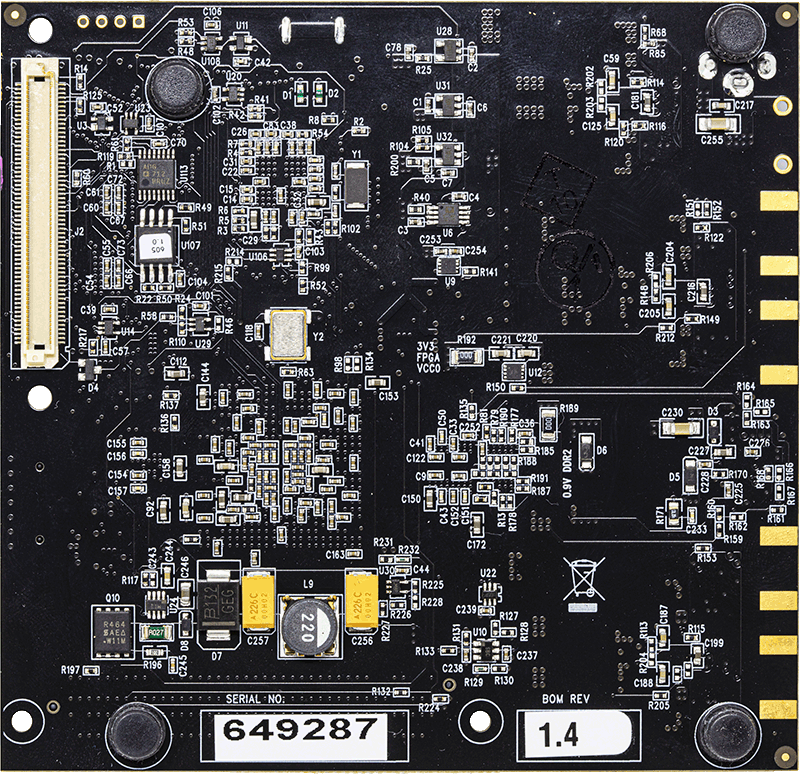
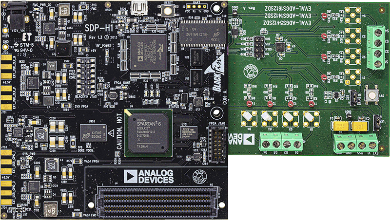
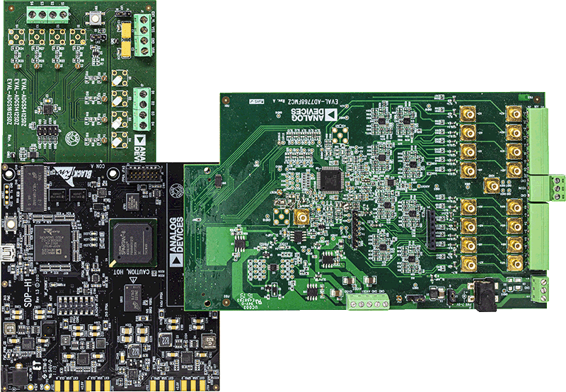
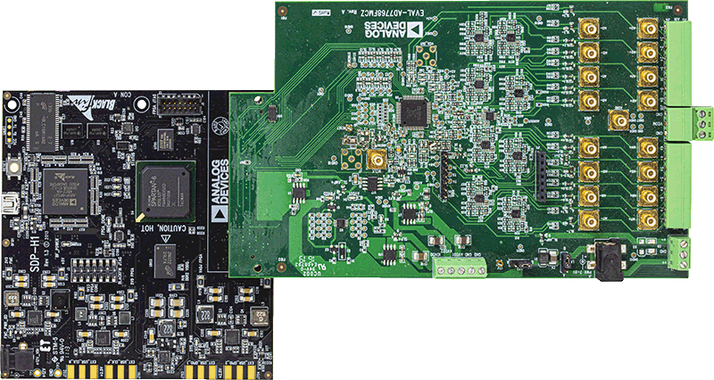
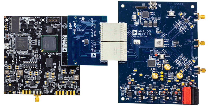
High Speed Controller Board
Resources
Software
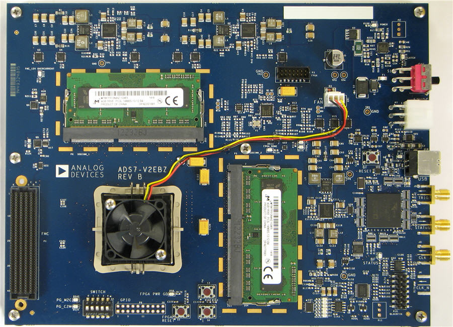
FPGA Based Data Capture Kit
Resources
Latest Discussions
No discussions on AD9148 yet. Have something to say?
Start a Discussion on EngineerZone®