AD6649
RECOMMENDED FOR NEW DESIGNSIF Diversity Receiver
- Part Models
- 2
- 1ku List Price
- Starting From $98.04
Part Details
- SNR = 73.0 dBFS in a 95 MHz BW at 185 MHz Ain and 245.76 MSPS
- SFDR = 85 dBc at 185 MHz Ain and 250 MSPS
- -151.2 dBFS/Hz Input Noise @ 220 MHz, -1dBFS Ain and 250MSPS
- 1.8 V analog and LVDS output supply operation
- Integer 1-to-8 input clock divider (625Mhz maximum input)
- Integrated dual-channel ADC
Sample rates up to 250 MSPS
IF sampling frequencies to 400 MHz
- Total Power consumption: 1W
- Integrated wideband digital downconverter (DDC)
32-bit complex, numerically controlled oscillator (NCO)
Sample Rate Converter and FIR filter with two modes
Real Output from an fs/4 output NCO - Fast detect bits for efficient AGC implementation
- Energy-saving power-down modes
- Decimated Interleaved ‘Real’ LVDS Data Outputs
- See datasheet for additional features
The AD6649 is a mixed-signal intermediate frequency (IF) receiver consisting of dual 14-bit, 250 MSPS ADCs and a wideband digital downconverter (DDC). The AD6649 is designed to support communications applications, where low cost, small size, wide bandwidth, and versatility are desired.
The dual ADC cores feature a multistage, differential pipelined architecture with integrated output error correction logic. Each ADC features wide bandwidth inputs supporting a variety of user-selectable input ranges. An integrated voltage reference eases design considerations. A duty cycle stabilizer is provided to compensate for variations in the ADC clock duty cycle, allowing the converters to maintain excellent performance.
ADC data outputs are internally connected directly to the digital downconverter (DDC) of the receiver. The digital receiver has two channels and provides processing flexibility. Each receive channel has four cascaded signal processing stages: a 32-bit frequency translator (numerically controlled oscillator (NCO)), an optional sample rate converter, a fixed FIR filter, and an fS/4 fixed-frequency NCO.
n addition to the receiver DDC, the AD6649 has several functions that simplify the automatic gain control (AGC) function in the system receiver. The programmable threshold detector allows monitoring of the incoming signal power using the fast detect output bits of the ADC. If the input signal level exceeds the programmable threshold, the fast detect indicator goes high. Because this threshold indicator has low latency, the user can quickly turn down the system gain to avoid an overrange condition at the ADC input.
After digital processing, data is routed directly to the 14-bit output port. These outputs operate at ANSI or reduced swing LVDS signal levels.
The AD6649 receiver digitizes a wide spectrum of IF frequencies. Each receiver is designed for simultaneous reception of the main channel and the diversity channel. This IF sampling architecture greatly reduces component cost and complexity compared with traditional analog techniques or less integrated digital methods. In diversity applications, the output data format is real due to the final NCO, which shifts the output center frequency to fS/4.
Flexible power-down options allow significant power savings, when desired.
Programming for setup and control is accomplished using a 3-pin SPI-compatible serial interface.
The AD6649 is available in a 64-lead LFCSP and is specified over the industrial temperature range of −40°C to +85°C. This product is protected by a U.S. patent.
Applications
- Communications
- Diversity radio systems
- Multimode digital receivers (3G)
TD-SCDMA, WiMax, WCDMA,
CDMA2000, GSM, EDGE, LTE - General-purpose software radios
- Broadband data applications
Product Highlights
- Integrated dual, 14-bit, 250 MSPS ADC.
- Integrated wideband decimation filter and 32-bit complex NCO.
- Fast overrange and threshold detect.
- Proprietary differential input maintains excellent SNR performance for input frequencies up to 300 MHz.
- SYNC input allows synchronization of multiple devices.
- 3-pin, 1.8V SPI port for register programming and register readback.
Documentation
Data Sheet 1
User Guide 1
Application Note 16
Evaluation Design File 3
ADI has always placed the highest emphasis on delivering products that meet the maximum levels of quality and reliability. We achieve this by incorporating quality and reliability checks in every scope of product and process design, and in the manufacturing process as well. "Zero defects" for shipped products is always our goal. View our quality and reliability program and certifications for more information.
| Part Model | Pin/Package Drawing | Documentation | CAD Symbols, Footprints, and 3D Models |
|---|---|---|---|
| AD6649BCPZ | 64-Lead LFCSP (9mm x 9mm w/ EP) | ||
| AD6649BCPZRL7 | 64-Lead LFCSP (9mm x 9mm w/ EP) |
| Part Models | Product Lifecycle | PCN |
|---|---|---|
|
Jul 27, 2020 - 20_0126 Conversion of Select Sizes LFCSP Products from Punched to Sawn and Transfer of Assembly Site to ASE Korea |
||
| AD6649BCPZ | PRODUCTION | |
| AD6649BCPZRL7 | PRODUCTION | |
This is the most up-to-date revision of the Data Sheet.
Software Resources
Can't find the software or driver you need?
Request a Driver/SoftwareHardware Ecosystem
| Parts | Product Life Cycle | Description |
|---|---|---|
| Clock ICs 9 | ||
| AD9510 | RECOMMENDED FOR NEW DESIGNS | 1.2 GHz Clock Distribution IC, PLL Core, Dividers, Delay Adjust, Eight Outputs |
| AD9511 | RECOMMENDED FOR NEW DESIGNS | 1.2 GHz Clock Distribution IC, PLL Core, Dividers, Delay Adjust, Five Outputs |
| AD9512 | RECOMMENDED FOR NEW DESIGNS | 1.2 GHz Clock Distribution IC, Two 1.6 GHz Inputs, Dividers, Delay Adjust, Five Outputs |
| AD9513 | RECOMMENDED FOR NEW DESIGNS | 800 MHz Clock Distribution IC, Dividers, Delay Adjust, Three Outputs |
| AD9514 | RECOMMENDED FOR NEW DESIGNS | 1.6 GHz Clock Distribution IC, Dividers, Delay Adjust, Three Outputs |
| AD9515 | RECOMMENDED FOR NEW DESIGNS | 1.6 GHz Clock Distribution IC, Dividers, Delay Adjust, Two Outputs |
| AD9523 | NOT RECOMMENDED FOR NEW DESIGNS | 14-Output, Low Jitter Clock generator |
| AD9523-1 | RECOMMENDED FOR NEW DESIGNS | Low Jitter Clock Generator with 14 LVPECL/LVDS/HSTL/29 LVCMOS Outputs |
| AD9524 | NOT RECOMMENDED FOR NEW DESIGNS | 6 Output, Dual Loop Clock Generator |
| Differential Amplifiers 3 | ||
| ADL5562 | RECOMMENDED FOR NEW DESIGNS | 3.3 GHz Ultralow Distortion RF/IF Differential Amplifier |
| ADA4927-2 | RECOMMENDED FOR NEW DESIGNS | Ultralow Distortion Current Feedback Differential ADC Driver |
| ADA4938-2 | RECOMMENDED FOR NEW DESIGNS | Ultralow Distortion Differential ADC Driver (Dual) |
| RF Amplifiers 1 | ||
| ADL5202 | Obsolete | Wide Dynamic Range, High Speed, Digitally Controlled VGA |
| RF VGAs (Variable Gain Amplifiers) 1 | ||
| AD8376 | RECOMMENDED FOR NEW DESIGNS | Ultralow Distortion IF Dual VGA |
Tools & Simulations
Virtual Eval - BETA
Virtual Eval is a web application to assist designers in product evaluation of ADCs, DACs, and other ADI products. Using detailed models on Analog’s servers, Virtual Eval simulates crucial part performance characteristics within seconds. Configure operating conditions such as input tones and external jitter, as well as device features like gain or digital down-conversion. Performance characteristics include noise, distortion, and resolution, FFTs, timing diagrams, response plots, and more.
Open ToolAD6649 IBIS Model 1
Visual Analog
For designers who are selecting or evaluating high speed ADCs, VisualAnalog™ is a software package that combines a powerful set of simulation and data analysis tools with a user-friendly graphical interface.
Open ToolADIsimRF
ADIsimRF is an easy-to-use RF signal chain calculator. Cascaded gain, noise, distortion and power consumption can be calculated, plotted and exported for signal chains with up to 50 stages. ADIsimRF also includes an extensive data base of device models for ADI’s RF and mixed signal components.
Open ToolS-Parameter 1
Evaluation Kits
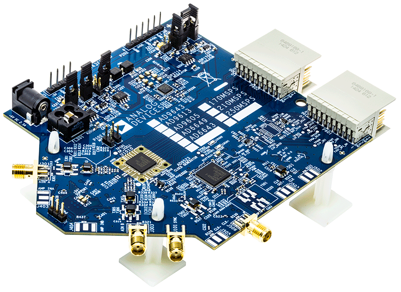
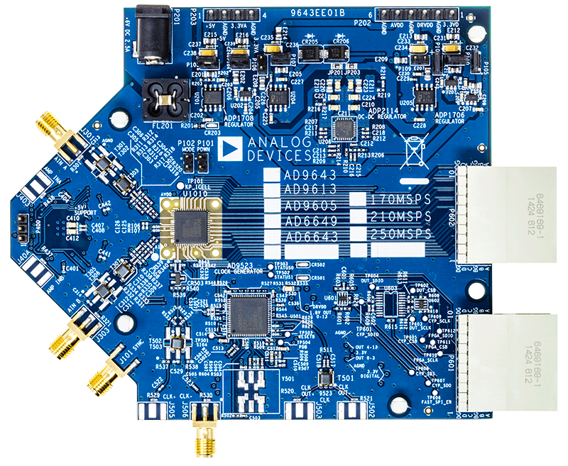
AD6649 Evaluation Board
Resources
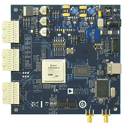
FPGA-Based Data Capture Kit
Resources
Software
Latest Discussions
No discussions on AD6649 yet. Have something to say?
Start a Discussion on EngineerZone®