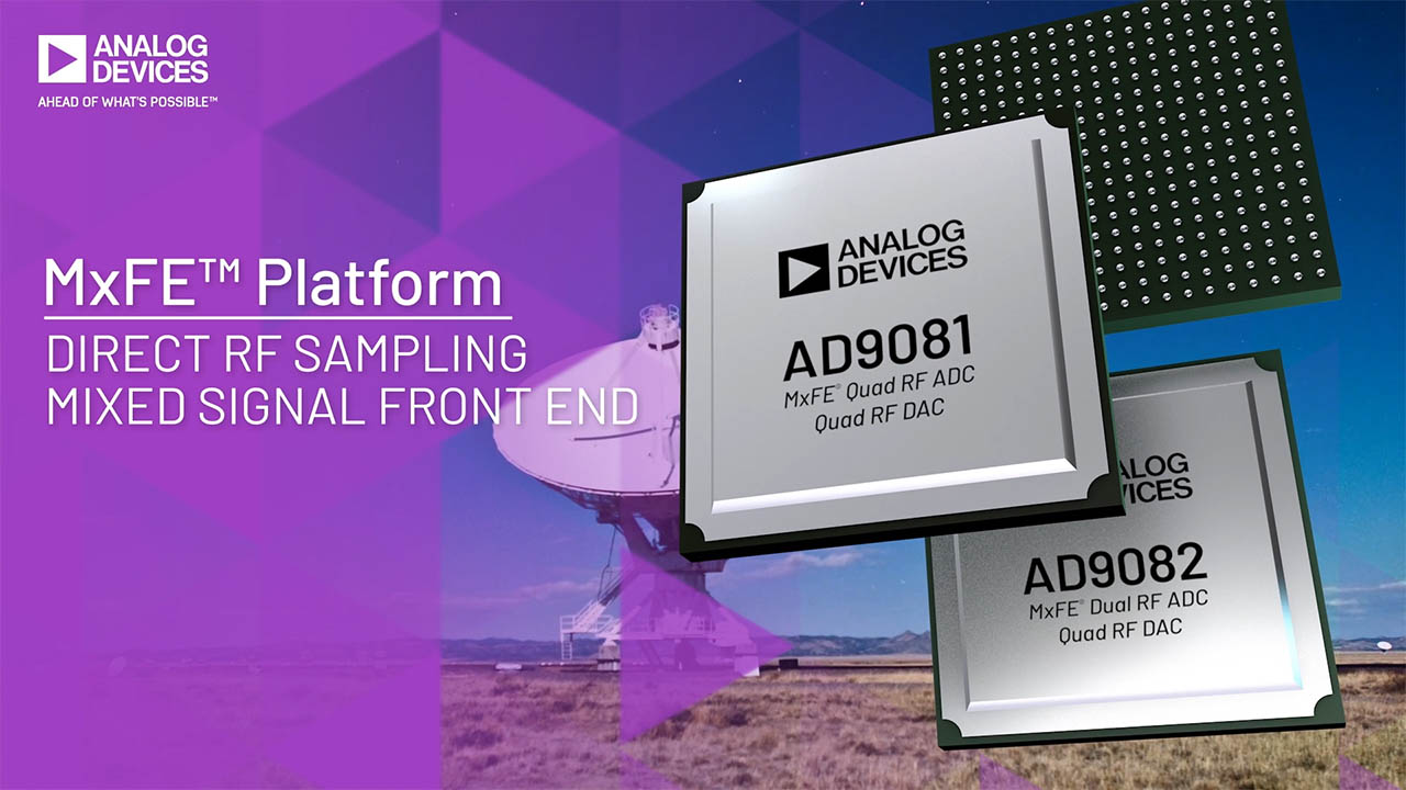
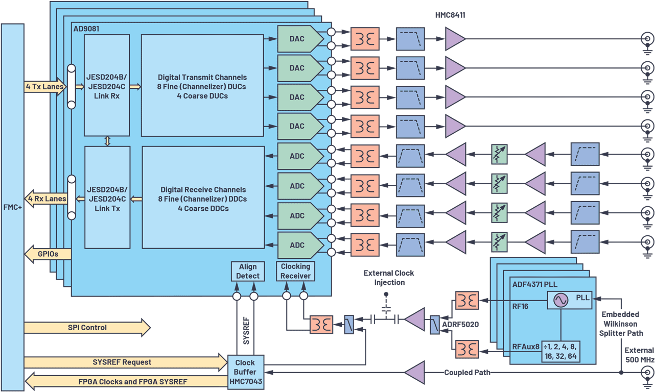
AD9081
RECOMMENDED FOR NEW DESIGNSMxFE™ Quad, 16-Bit, 12GSPS RFDAC and Quad, 12-Bit, 4GSPS RFADC
- Part Models
- 4
- 1ku List Price
- Starting From $1177.00
Part Details
- Flexible, reconfigurable common platform design
- 4 DACs and 4 ADCs (4D4A)
- Supports single, dual, and quad band
- Datapaths and DSP blocks are fully bypassable
- DAC to ADC sample rate ratios of 1, 2, 3, and 4
- On-chip PLL with multichip synchronization
- External RFCLK input option for off-chip PLL
- Maximum DAC sample rate up to 12 GSPS
- Maximum data rate up to 12 GSPS using JESD204C
- Useable analog bandwidth to 8 GHz
- Maximum ADC sample rate up to 4 GSPS
- Maximum data rate up to 4 GSPS using JESD204C
- 7.5 GHz analog input full power bandwidth (−3 dB)
- ADC ac performance at 4 GSPS, input at −2.7 GHz, −1 dBFS
- Full-scale input voltage: 1.4 V p-p
- Noise density: −147.5 dBFS/Hz
- Noise figure: 26.8 dB
- HD2: −67 dBFS
- HD3: −73 dBFS
- Worst other (excluding HD2 and HD3): −79 dBFS at 2.7 GHz
- DAC ac performance at 12 GSPS
- Full-scale output current range: 6.43 mA to 37.75 mA
- Two-tone IMD3 (−7 dBFS per tone): −78.9 dBc
- NSD, single-tone at 3.7 GHz: −155.1 dBc/Hz
- SFDR, single-tone at 3.7 GHz: −70 dBc
- SERDES JESD204B/JESD204C interface, 16 lanes up to 24.75 Gbps
- 8 lanes JESD204B/C transmitter (JTx) and 8 lanes JESD204B/C receiver Rx (JRx)
- JESD204B compliance with the maximum 15.5 Gbps
- JESD204C compliance with the maximum 24.75 Gbps
- Supports real or complex digital data (8-, 12-, 16-, or 24-bit)
- Versatile digital features
- Configurable or by-passable DDCs and DUCs
- 8 fine complex DUCs and 4 coarse complex DUCs
- 8 fine complex DDCs and 4 coarse complex DDCs
- 48-bit NCO per DUC or DDC
- Programmable 192-tap PFIR filter for receive equalization
- Supports 4 different profile settings loaded via GPIO
- Programmable delay per datapath
- Receive AGC support
- Fast detect with low latency for fast AGC control
- Signal monitor for slow AGC control
- Transmit DPD support
- Fine DUC channel gain control and delay adjust
- Coarse DDC delay adjust for DPD observation path
- Auxiliary features
- Fast frequency hopping and direct digital synthesis (DDS)
- Low latency loopback mode (receive datapath data can be routed to the transmit datapaths)
- ADC clock driver with selectable divide ratios
- Power amplifier downstream protection circuitry
- On-chip temperature monitoring unit
- Flexible GPIO pins
- TDD power savings option and sharing ADCs
- 15 mm × 15 mm, 324-ball BGA with 0.8 mm pitch
The AD9081 mixed signal front end (MxFE®) is a highly integrated device with four 16-bit, 12 GSPS maximum sample rate, RF digital-to-analog converter (DAC) cores, and four 12-bit, 4 GSPS rate, RF analog-to-digital converter (ADC) cores. The AD9081 is well suited for applications requiring both wideband ADCs and DACs to process signal(s) that have wide instantaneous bandwidth. The device features eight transmit and eight receive lanes that support 24.75 Gbps/lane JESD204C or 15.5 Gbps/lane JESD204B standards. The device also has an on-chip clock multiplier, and a digital signal processing (DSP) capability targeted at either wideband or multiband direct to RF applications. The DSP datapaths can be bypassed to allow a direct connection between the converter cores and the JESD204 data transceiver port. The device also features low latency loopback and frequency hopping modes targeted at phase array radar system and electronic warfare applications. Two models for the AD9081 are offered. The 4D4AC model supports the full instantaneous channel bandwidth, whereas the 4D4AB model supports a maximum instantaneous bandwidth of 600 MHz per channel by automatically configuring the DSP to limit the instantaneous bandwidth at startup.
APPLICATIONS
- Wireless communications infrastructure
- Microwave point-to-point, E-band and 5G mmWave
- Broadband communications systems
- DOCSIS 3.1 and 4.0 CMTS
- Phased array radar and electronic warfare
- Electronic test and measurement systems
Documentation
Data Sheet 1
User Guide 2
Application Note 1
Design Note 1
Technical Articles 12
Video 12


FPGA Interoperability Reports 5
Device Drivers 2
Product Selection Guide 1
3rd Party Solutions 1
Analog Dialogue 3
Video Series 1
Webcast 1
ADI has always placed the highest emphasis on delivering products that meet the maximum levels of quality and reliability. We achieve this by incorporating quality and reliability checks in every scope of product and process design, and in the manufacturing process as well. "Zero defects" for shipped products is always our goal. View our quality and reliability program and certifications for more information.
| Part Model | Pin/Package Drawing | Documentation | CAD Symbols, Footprints, and 3D Models |
|---|---|---|---|
| AD9081BBPZ-4D4AB | 324-Ball BGA_ED (15mm x 15mm x 1.58mm) | ||
| AD9081BBPZ-4D4AC | 324-Ball BGA_ED (15mm x 15mm x 1.58mm) | ||
| AD9081BBPZRL-4D4AB | 324-Ball BGA_ED (15mm x 15mm x 1.58mm) | ||
| AD9081BBPZRL-4D4AC | 324-Ball BGA_ED (15mm x 15mm x 1.58mm) |
This is the most up-to-date revision of the Data Sheet.
Software Resources
Device Drivers 3
- AD9081 GitHub no-OS Driver Source Code
- AD908x GitHub Linux Driver Source Code
API Device Drivers 1
Device Application Programming Interface (API) C code drivers provided as reference code that allows the user to quickly configure the product using high-level function calls. The library acts as an abstraction layer between the application and the hardware. The API is developed in C99 to ensure agnostic processor and operating system integration. Customers can port this application layer code to their embedded systems by integrating their platform-specific code base to the API HAL layer.
To request this software package, go to the Software Request Form signed in with your MyAnalog account and under “Target Hardware” select “High Speed Data Converters” and choose the desired API product package. You will receive an email notification once the software is provided to you.
Evaluation Software 1
JESD204x Frame Mapping Table Generator
The JESD204x Frame Mapping Table Generator tool consists of two Windows executables that will allow the user to input any valid combination of JESD204x parameters (L, M, F, S, NP) in order to output a .csv file that illustrates the frame mapping of the JESD204x mode in table format. There is an executable that allows the user to input a single JESD204x mode and another, that allows the user to input the parameters for multiple JESD204x modes in a specified .csv format in order to output a .csv file that illustrates the frame mapping of each of the JESD204x modes that were input into separate tables.
Hardware Ecosystem
| Parts | Product Life Cycle | Description |
|---|---|---|
| Clock ICs 3 | ||
| LTC6953 | LAST TIME BUY | Ultralow Jitter, 4.5GHz Clock Distributor with 11 Outputs and JESD204B/JESD204C Support |
| LTC6952 | LAST TIME BUY | Ultralow Jitter, 4.5GHz PLL with 11 Outputs and JESD204B / JESD204C Support |
| HMC7044 | RECOMMENDED FOR NEW DESIGNS | High Performance, 3.2 GHz, 14-Output Jitter Attenuator with JESD204B and JESD204C Support |
| Differential Amplifiers 2 | ||
| ADL5569 | RECOMMENDED FOR NEW DESIGNS | 6.5 GHz, Ultrahigh Dynamic Range, Differential Amplifier |
| ADL5580 | RECOMMENDED FOR NEW DESIGNS | Fully Differential, 10 GHz ADC Driver with 10 dB Gain |
| Fanout Buffers & Splitters 2 | ||
| HMC7043 | RECOMMENDED FOR NEW DESIGNS |
High Performance, 3.2 GHz, 14-Output Fanout Buffer with JESD204B/JESD204C |
| LTC6955 | LAST TIME BUY | Ultralow Jitter, 7.5GHz, 11 Output Fanout Buffer Family |
| LDO Linear Regulators 4 | ||
| ADP1765 | RECOMMENDED FOR NEW DESIGNS | 5 A, Low VIN, Low Noise, CMOS Linear Regulator |
| ADP7158 | RECOMMENDED FOR NEW DESIGNS | 2 A, Ultralow Noise, High PSRR, Fixed Output, RF Linear Regulator |
| ADM7172 | RECOMMENDED FOR NEW DESIGNS | 6.5 V, 2 A, Ultralow Noise, High PSRR, Fast Transient Response CMOS LDO |
| ADM7150 | RECOMMENDED FOR NEW DESIGNS | 800 mA, Ultra Low Noise/High PSRR LDO |
| Phase-Locked Loop (PLL) Synthesizers 1 | ||
| ADF4377 | RECOMMENDED FOR NEW DESIGNS | Microwave Wideband Synthesizer with Integrated VCO |
| RF VGAs (Variable Gain Amplifiers) 2 | ||
| ADL6316 | RECOMMENDED FOR NEW DESIGNS | 500 MHz to 1000 MHz Transmit VGA for Use with RF DACs and Transceivers |
| ADL6317 | RECOMMENDED FOR NEW DESIGNS | Transmit VGA for Use with RF DACs and Transceivers |
| Switching Regulators & Controllers 5 | ||
| LTM4633 | RECOMMENDED FOR NEW DESIGNS | Triple 10A Step-Down DC/DC μModule (Power Module) Regulator |
| LTM8053 | RECOMMENDED FOR NEW DESIGNS | 40VIN, 3.5A/6A Step-Down Silent Switcher μModule Regulator |
| LTM8063 | RECOMMENDED FOR NEW DESIGNS | 40VIN, 2A Silent Switcher µModule Regulator |
|
LTM4644 LTM4644-1 |
Quad DC/DC μModule (Power Module) Regulator with Configurable 4A Output Array | |
| LTM4616 | RECOMMENDED FOR NEW DESIGNS | Dual 8A per Channel Low VIN DC/DC μModule (Power Module) Regulator |
Tools & Simulations
ADC Companion Transport Layer RTL Code Generator Tool
This command line executable tool generates a Verilog module which implements the JESD204 receive transport layer. The user specifies in a configuration file one or more modes to be supported by the transport layer module. These modes are defined as a set of JESD204 parameter values: L, M, F, S, N', and CF. The transport layer converts JESD204 lane data output from a JESD204 link layer IP to a data bus with a fixed width, containing interleaved virtual converter samples. Both JESD204B and JESD204C link layers are supported.
Open ToolMxFE JESD204 Mode Selector Tool
The JESD204B/C Mode Selector Tool is a simple command line-based Windows executable that can be used to narrow down the number of JESD204x modes to only include those modes that support the user’s specific application use case. The tool guides the user through a use case description flow chart and gives the user a small list of applicable transmit and/or receive modes to choose from. This tool is applicable to the AD9081, AD9082, AD9177, AD9207, AD9209, AD9986, and AD9988.
Open ToolADIsimPLL™
ADIsimPLL enables the rapid and reliable evaluation of new high performance PLL products from ADI. It is the most comprehensive PLL Synthesizer design and simulation tool available today. Simulations performed include all key non-linear effects that are significant in affecting PLL performance. ADIsimPLL removes at least one iteration from the design process, thereby speeding the design- to-market.
Open ToolDAC Companion Transport Layer RTL Code Generator
These command line executable tool generates a Verilog module which implements the JESD204 transmitter transport layer. The user specifies in a configuration file one or more modes to be supported by the transport layer module. These modes are defined as a set of JESD204 parameter values: L, M, F, S, N', and CF. The transport layer converts JESD204 lane data output from a JESD204 link layer IP to a data bus with a fixed width, containing interleaved virtual converter samples. Both JESD204B and JESD204C link layers are supported.
Open ToolS-Parameter 2
High Speed Converter Toolbox for MATLAB
Open ToolIBIS Model 1
AD9081/AD9082/AD9986/AD9988 AMI Model
Open ToolThermal Models 1
Evaluation Kits
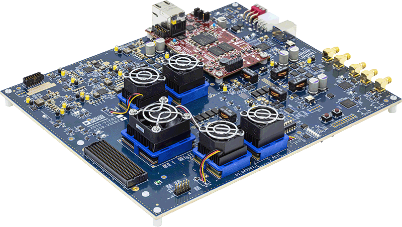
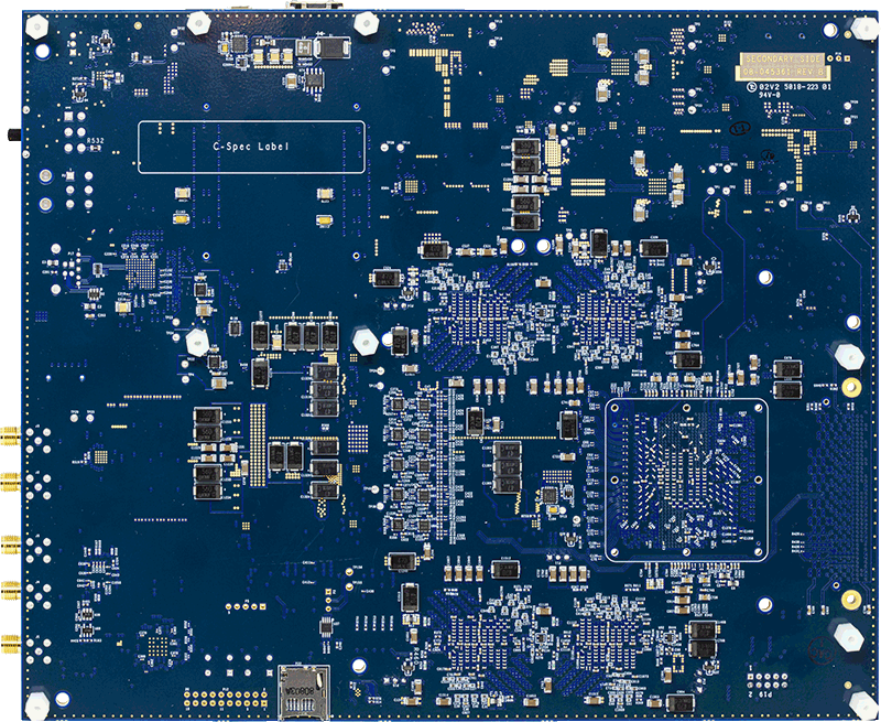
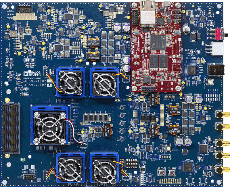
ADS9-V2EBZ Evaluation Board
Resources
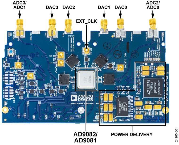
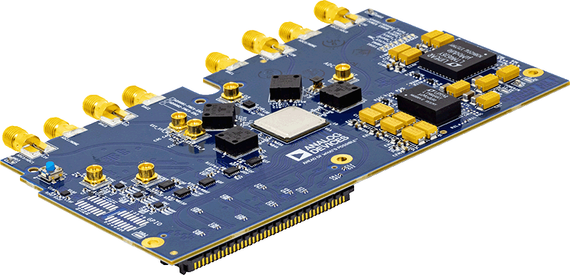
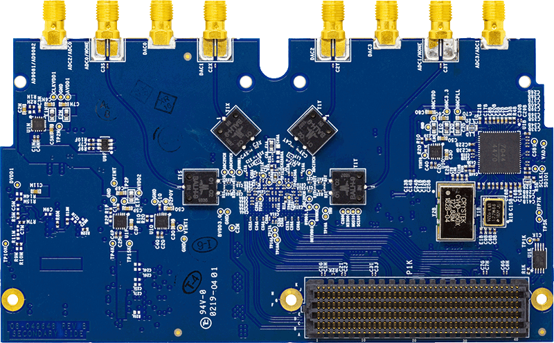
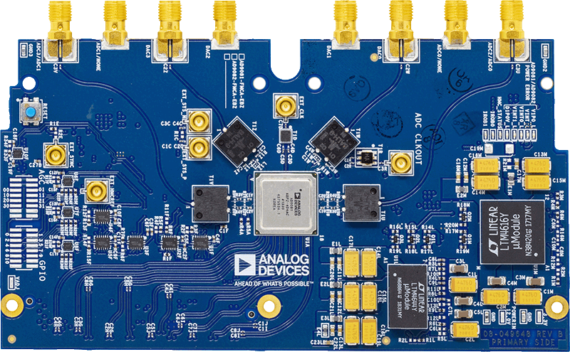
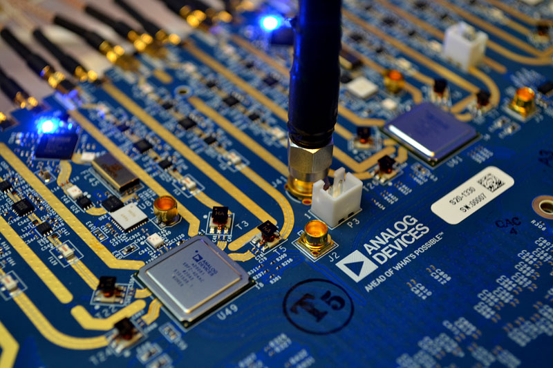
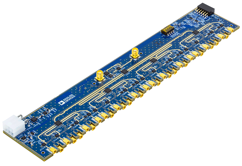
AD9081 Evaluation Board
Resources
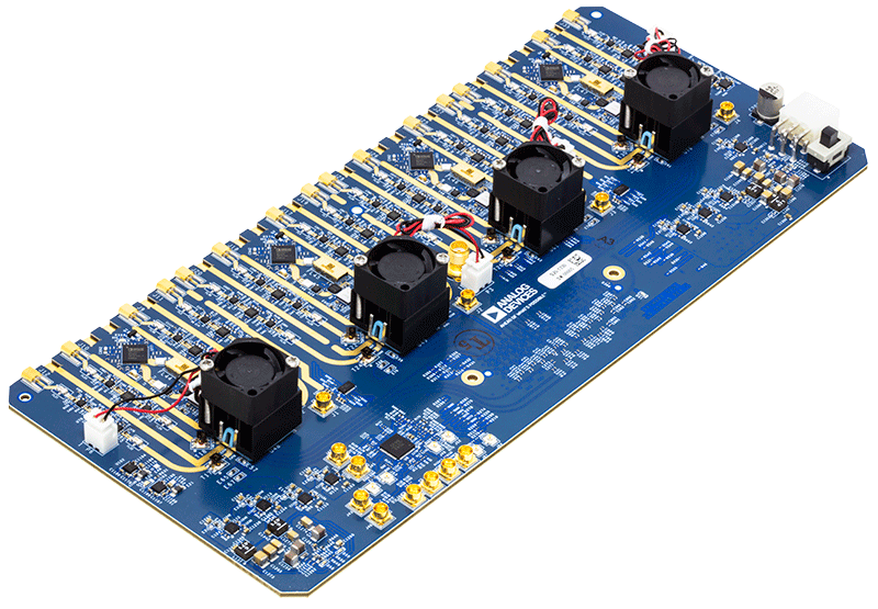
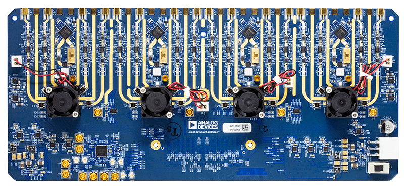
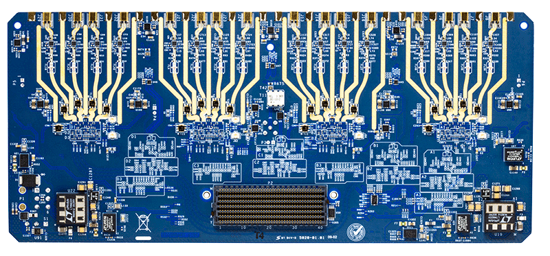
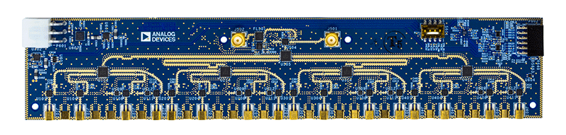
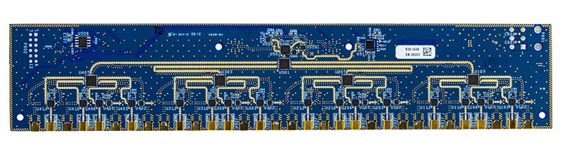
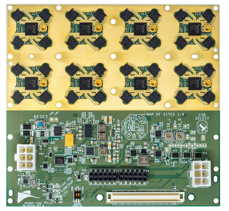
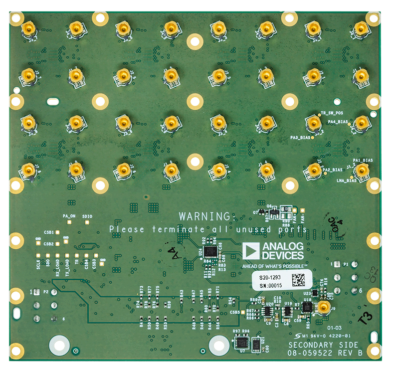
16Tx/16Rx Direct L/S/C-Band Sampled Phased-Array/RADAR/EW/SATCOM Development Platform
Resources
Software
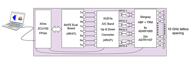
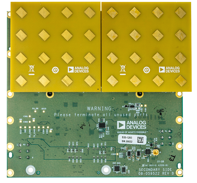
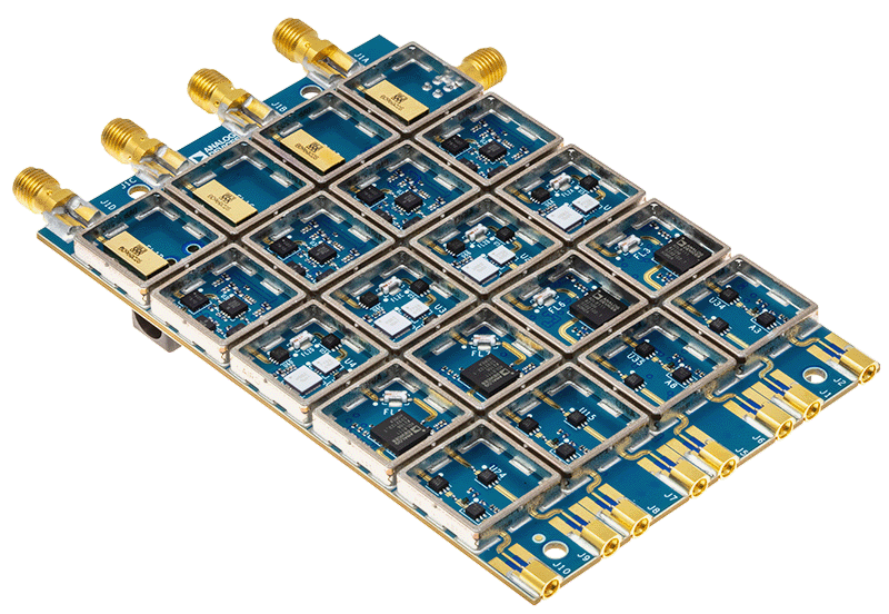
Scalable 32 Element Hybrid Beamforming Phased-Array RADAR Development Platform
Resources
Latest Discussions
No discussions on AD9081 yet. Have something to say?
Start a Discussion on EngineerZone®