
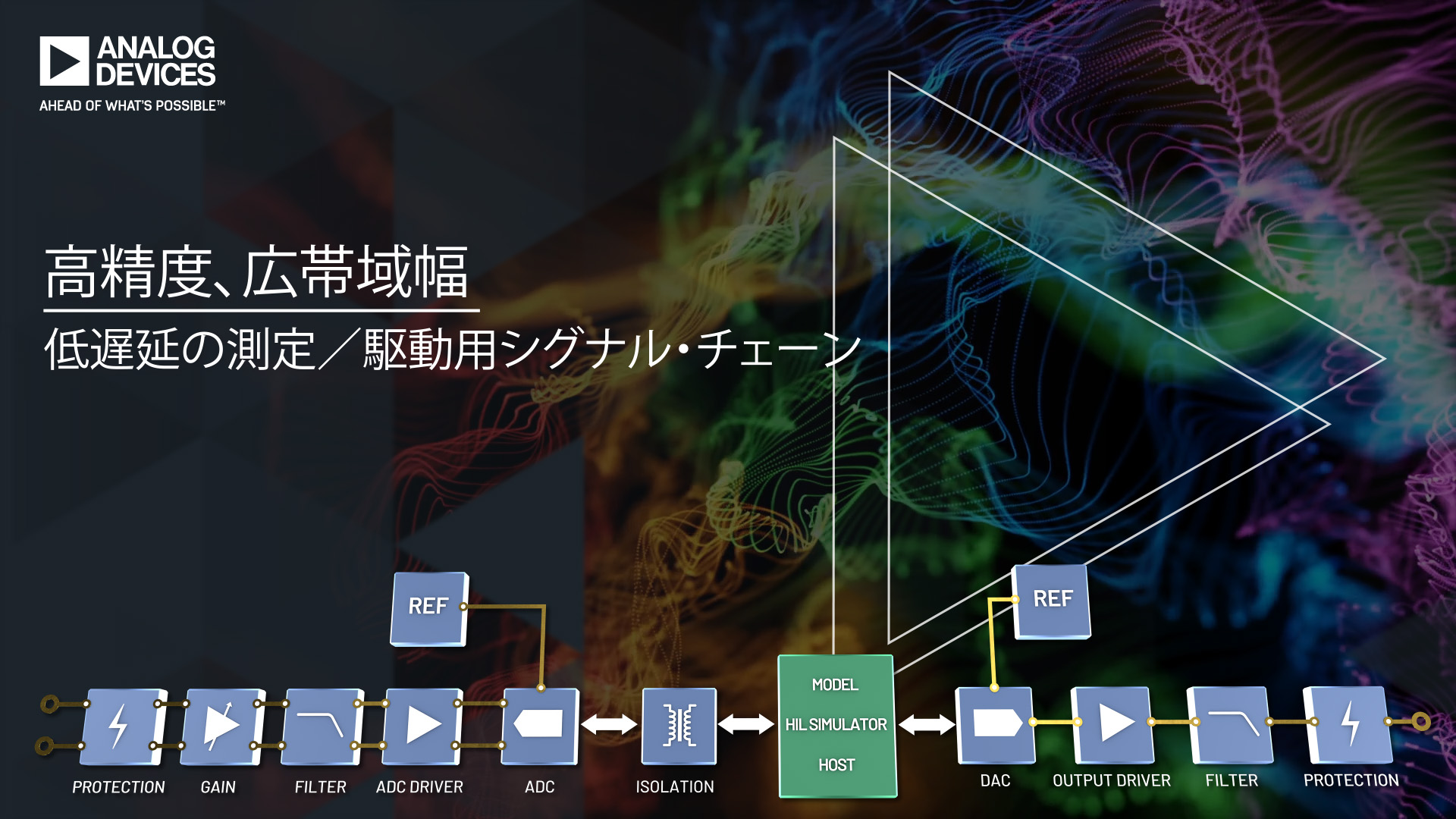
Save time and deliver your solutions faster with ADI’s new suite of precision technology signal chains. Align your applications ranging from Smart Industry to Instrumentation, Electrification to Digital Health, to exactly the right precision technology combinations.
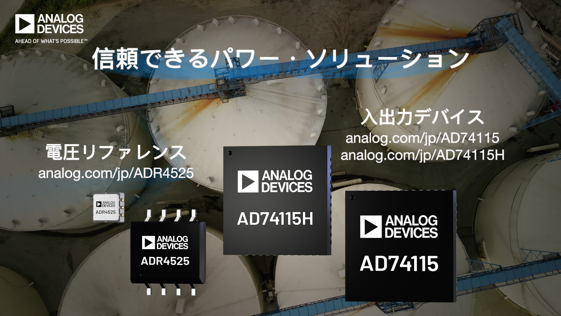
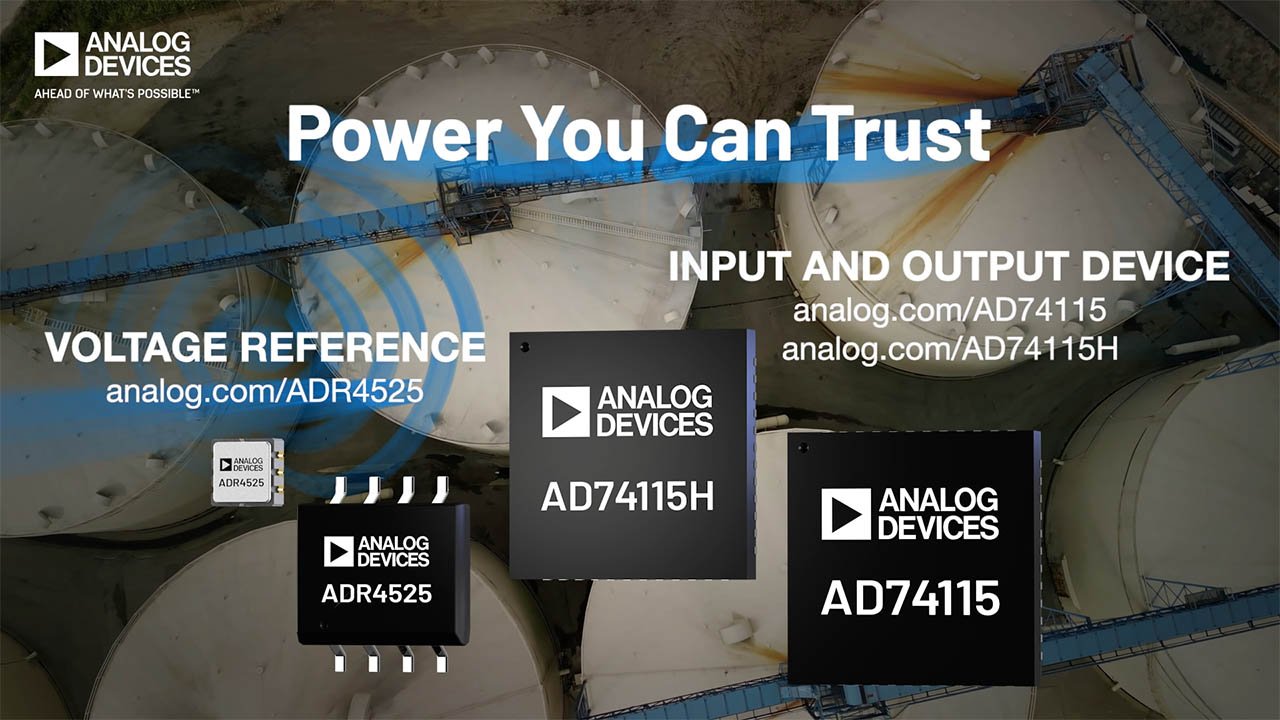
Tailor your signal chain with confidenceADR4525
新規設計に推奨2.5V電圧リファレンス、超低ノイズ、高精度
- 製品モデル
- 9
- 1Ku当たりの価格
- 最低価格:$2.89
製品の詳細
- 最大温度係数(TCVOUT):
- 0.8ppm / °C(Dグレード、0°C~70°C)
- 1ppm / °C(Cグレード、0°C~70°C)
- 2ppm / °C(Bグレード、−40°C~+125°C)
- 4ppm / °C(Aグレード、−40°C~+125°C)
- 出力ノイズ(0.1~10Hz):
- 2.048V(typ)のVOUT で1μVp-p
- 初期出力電圧誤差:
- B、C、Dグレード:±0.02%(最大)
- 入力電圧範囲:3~15V
- 動作温度:
- AグレードおよびBグレード:−40°C~+125°C
- CグレードおよびDグレード:0°C~+70°C
- 出力電流:+10mAソース/ -10mAシンク
- 低静止電流:950μA (max)
- 低ドロップアウト電圧:2mAで300mV(VOUT ≥ 3V)
- 8ピンSOICおよびLCCパッケージ
- AEC-Q100準拠により、自動車用アプリケーションに対応
- 長期ドリフト:4500時間で8ppm(代表値)
ADR4520/ADR4525/ADR4530/ADR4533/ADR4540/ADR4550のデバイスは、高精度、低消費電力、低ノイズの電圧リファレンスであり、± 0.02%(B、CまたはDグレード)の最大初期誤差、優れた温度安定性、低出力ノイズを持っています。
このファミリーの電圧リファレンスでは、高精度用の新しいコア回路を採用し、業界をリードする温度安定性とノイズ性能を提供しています。 また、このデバイスの出力電圧熱ヒステリシスは小さく、かつ長期出力電圧ドリフトも小さいため、時間と温度変動に対するシステム精度を向上させることができます。
最大動作電流は950μAで、かつ最大300mVの低ドロップアウト電圧なので、このデバイスは携帯型装置で使用することができます。
電圧リファレンスのADR4520/ADR4525/ADR4530/ADR4533/ADR4540/ADR4550 シリーズは広範囲な出力電圧を持ち、8ピンSOICを採用し、全デバイスとも仕様は−40°C~+125°Cの拡張工業用温度範囲で規定されています
ADR4525、ADR4540、ADR4550は、温度範囲が0℃~70℃であるDグレード(8ピンLCCパッケージで提供)とCグレードでも利用可能です。ADR4525W(8ピンSOICパッケージを採用)は車載アプリケーション向けに性能評価済みです。
アプリケーション
- 高精度データ・アクイジション・システム
- 高分解能データ・コンバータ
- 高精度計測機器
- 工業用計装機器
- 医用機器
- 車載バッテリのモニタリング
ドキュメント
データシート 2
アプリケーション・ノート 3
技術記事 1
よく聞かれる質問 1
ビデオ 8


サードパーティ・ソリューション 1
リファレンス設計 4
Analog Dialogue 1
| 製品モデル | ピン/パッケージ図 | 資料 | CADシンボル、フットプリント、および3Dモデル |
|---|---|---|---|
| ADR4525ARZ | 8-Lead SOIC | ||
| ADR4525ARZ-R7 | 8-Lead SOIC | ||
| ADR4525BRZ | 8-Lead SOIC | ||
| ADR4525BRZ-R7 | 8-Lead SOIC | ||
| ADR4525CRZ | 8-Lead SOIC | ||
| ADR4525CRZ-R7 | 8-Lead SOIC | ||
| ADR4525DEZ | LCC:CER LEADLESS CHIP CARR | ||
| ADR4525DEZ-R7 | LCC:CER LEADLESS CHIP CARR | ||
| ADR4525WBRZ-R7 | 8-Lead SOIC |
これは最新改訂バージョンのデータシートです。
ハードウェア・エコシステム
| 製品モデル | 製品ライフサイクル | 詳細 |
|---|---|---|
| LDO Linear Regulators 1 | ||
| LT3040 | 新規設計に推奨 | 20V、200mA、超低ノイズ、超高PSRR高精度DAC/リファレンス・バッファ |
ツールおよびシミュレーション
LTspice 1
下記製品はLTspiceで使用することが出来ます。:
- ADR4525
Signal Chain Designer – BETA版
Signal Chain Designerは、複雑な高精度シグナル・チェーンの構築、シミュレーションを行うために設計されたウェブベースのツールです。PCBを作成する前に、伝達関数、ノイズ、消費電力、入力範囲、DCエラーなど、回路の性能を確認できます。さまざまな部品やアーキテクチャを素早く試すことができます。シグナル・チェーンはLTspiceにエクスポートして更に解析を行うことができます。
ツールを開く
LTspice®は、無料で提供される強力で高速な回路シミュレータと回路図入力、波形ビューワに改善を加え、アナログ回路のシミュレーションを容易にするためのモデルを搭載しています。
評価用キット

Evaluation Board for the AD5676R WLCSP
資料
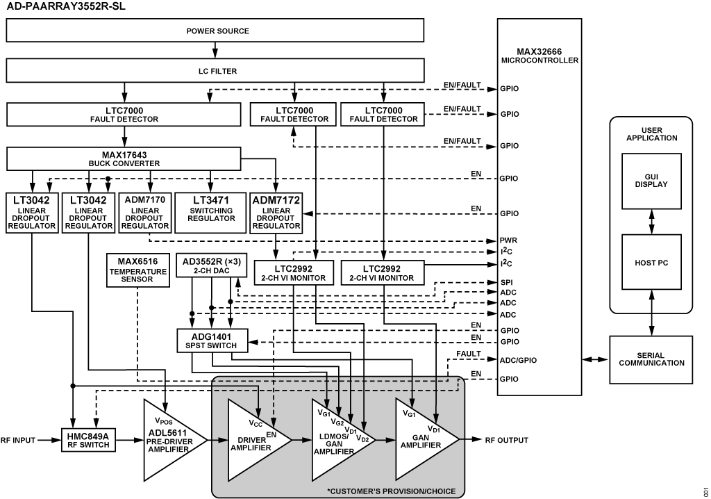
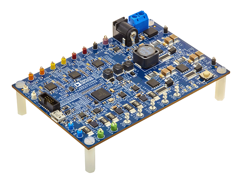
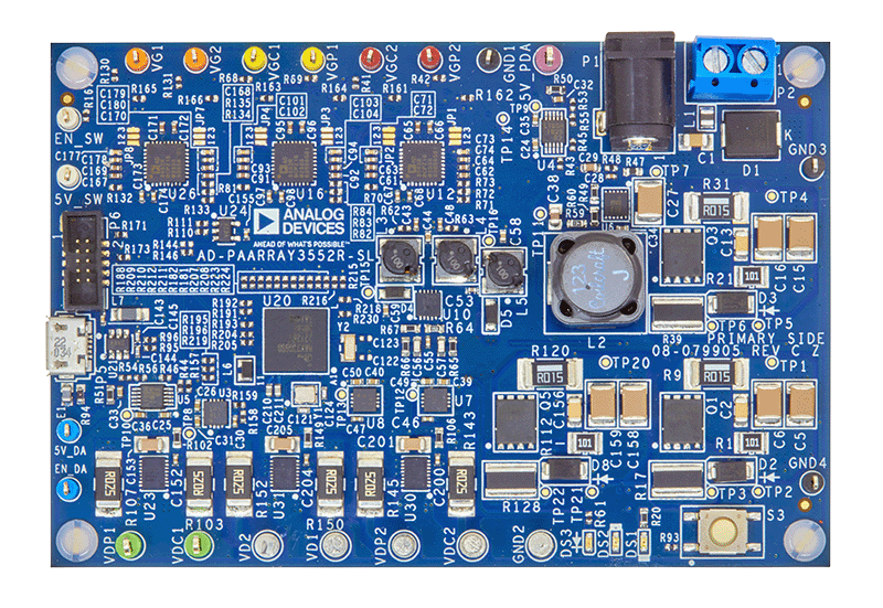
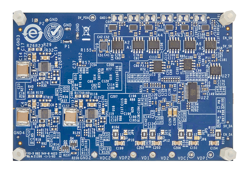
RF Front-end GaN Power Amplifier Biasing, Protection, and Control Reference Design
資料
ソフトウェア
リファレンス・デザイン
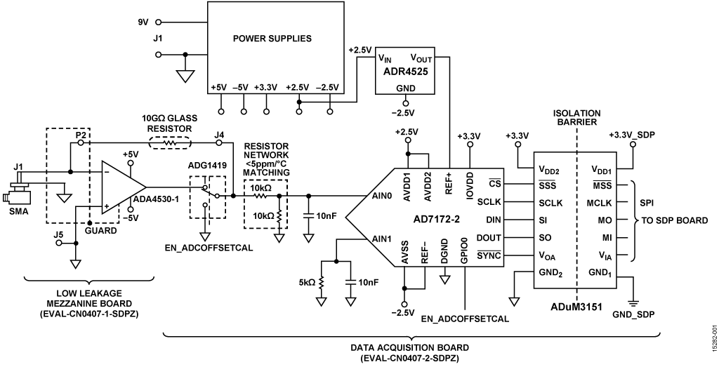
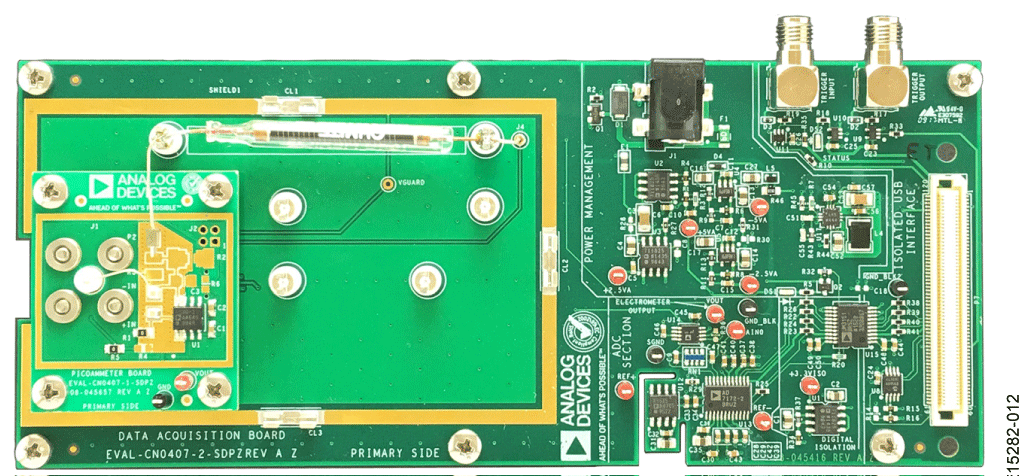
超高感度フェムトアンペア計測プラットフォーム ※Rev.0を翻訳したものです。最新版は英語資料をご覧ください。
使用製品
設計および組み込みツール
ビデオ
-
 sample_iTunes

-
Valeria
-
AnalogDevices-F04
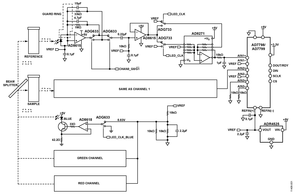
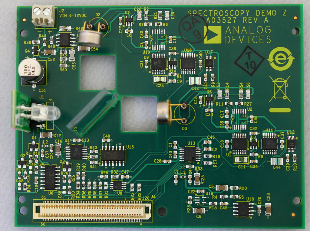
プログラマブル・ゲイン・トランスインピーダンス・アンプと同期検波器付き2チャンネル色度計 ※Rev.0を翻訳したものです。新ver.は英語資料をご覧ください。
使用製品
資料
設計および組み込みツール
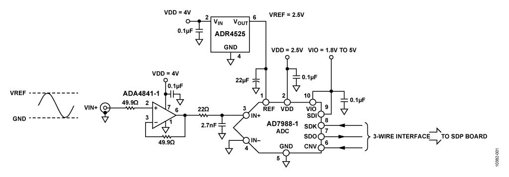

16 ビット、100kSPS、単電源、低消費電力データ・アクイジション・システム ※Rev.Aを翻訳したものです。最新版は英語資料をご覧ください。
使用製品
設計および組み込みツール
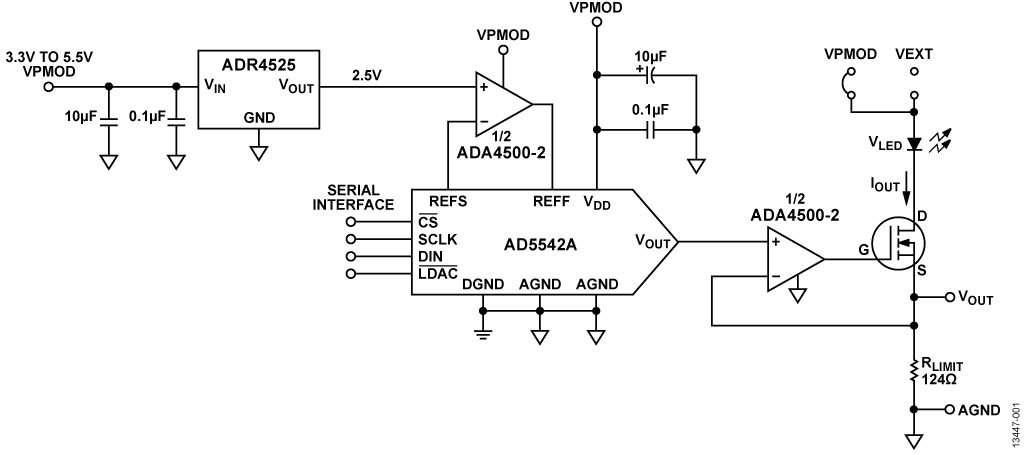
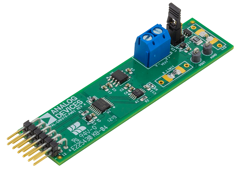
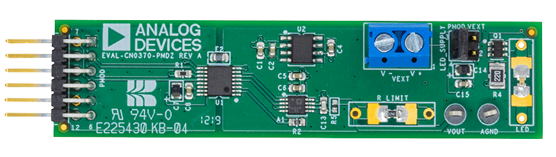
積分非直線性と微分非直線性が ±1 LSB 未満の 16 ビット、単電源 LED 電流ドライバ ※Rev.0を翻訳したものです。最新版は英語資料をご覧ください。
使用製品
設計および組み込みツール


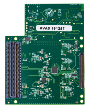
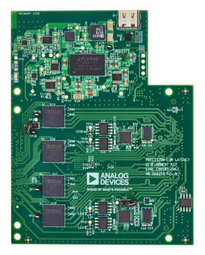
Quad Channel, Low Latency, Data Acquisition and Signal Generation Module
使用製品
資料
設計および組み込みツール
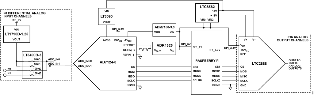
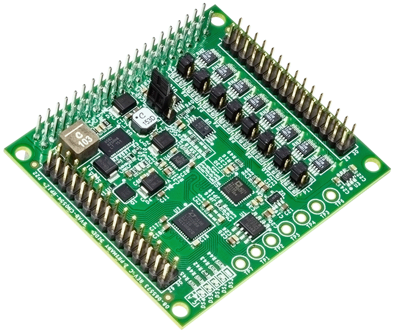
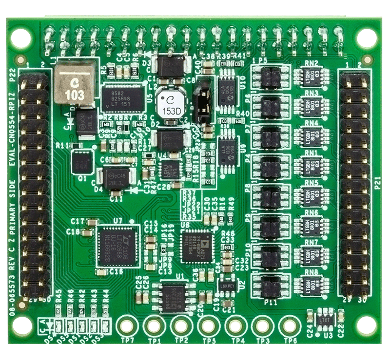

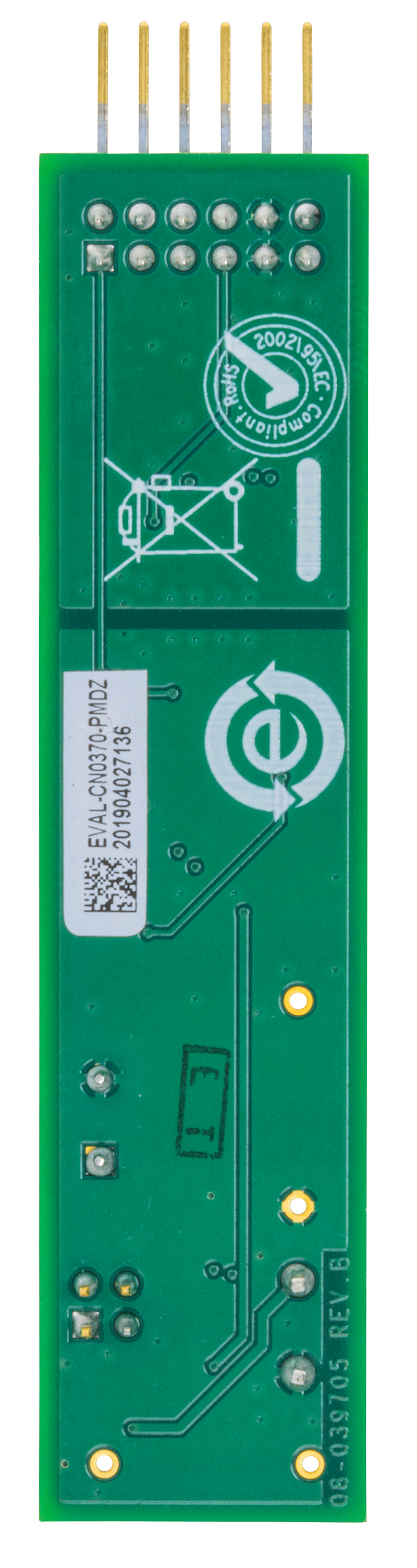
Raspberry Pi プラットフォーム対応±10V アナログ入力および±15V アナログ出力
使用製品
資料
設計および組み込みツール
ビデオ
-
CN0554: 10V Analog Input and 15V Analog Output for Raspberry Pi
最新のディスカッション
ADR4525に関するディスカッションはまだありません。意見を投稿しますか?
EngineerZone®でディスカッションを始める