Power

- Battery Monitors & Fuel Gauges
- Charge Pumps
- Circuit Monitors
- Lamp & Tube Drivers
- LED ドライバ IC
- Linear Regulators
- MOSFET & Gate Drivers
- PoE(Power-over-Ethernet)インターフェース・コントローラ
- Power System Managers & Sequencers
- Protection Switches & Controllers
- PWM & TEC Controllers
- Supervisors & Resets
- スイッチング・レギュレータ
- バッテリ・チャージャIC
- バッテリ管理
- ホットスワップコントローラ
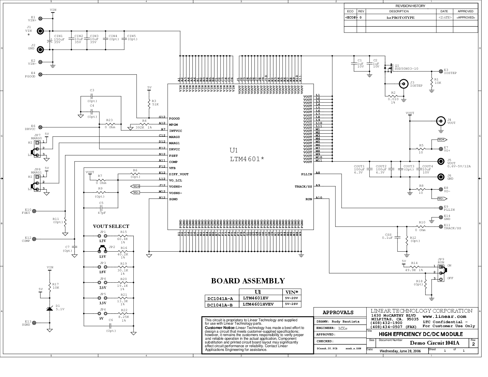
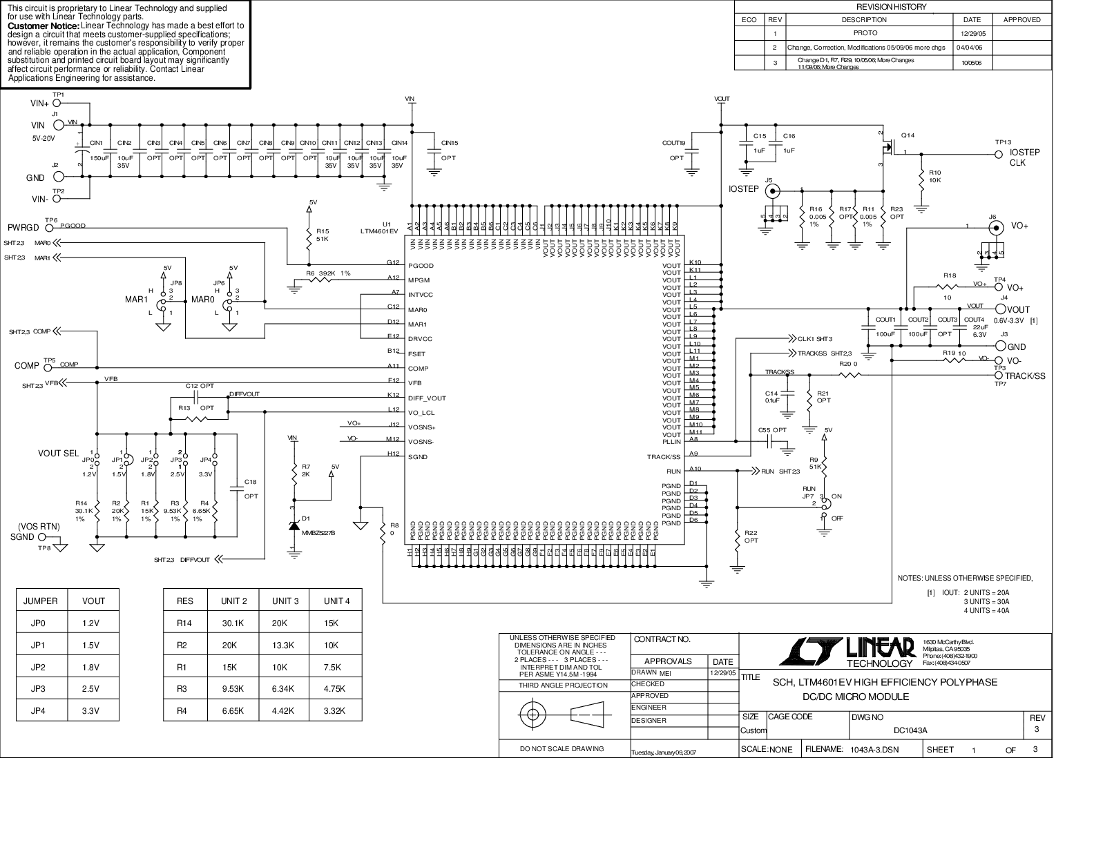
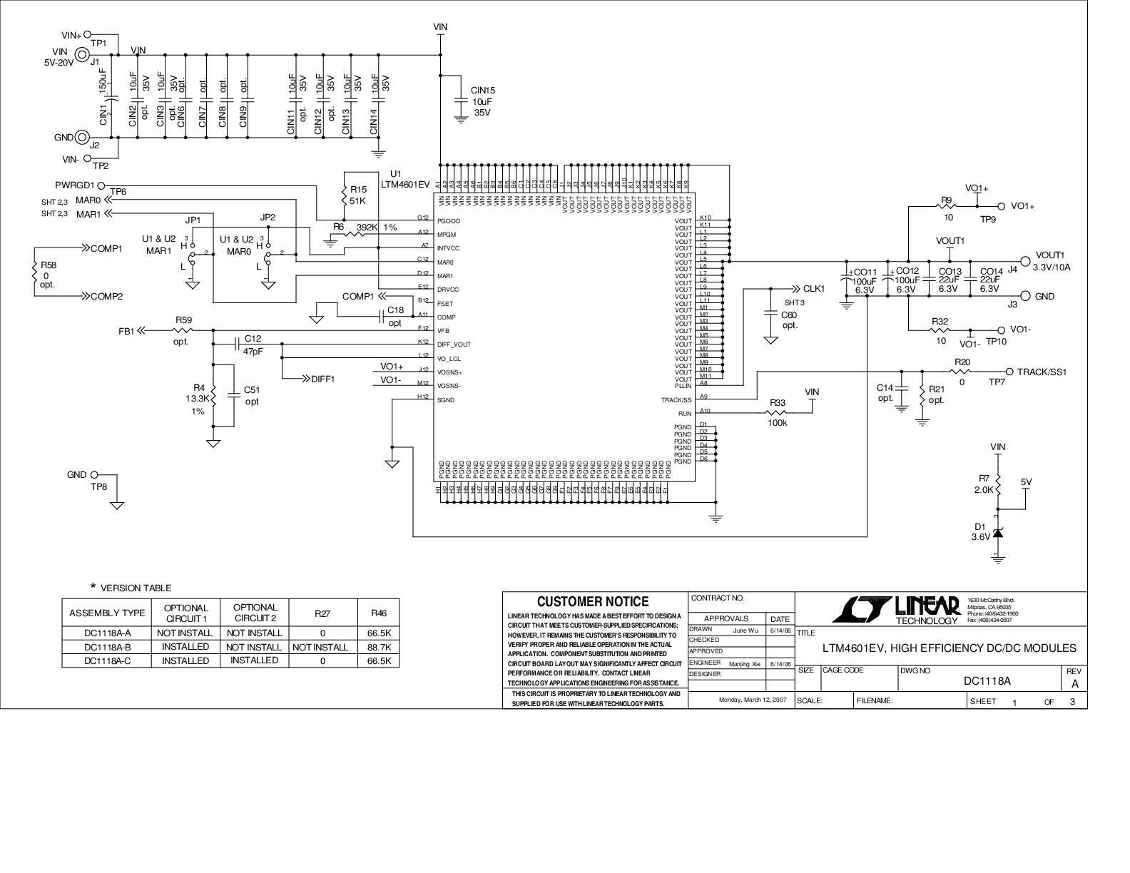
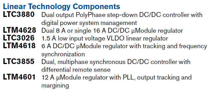
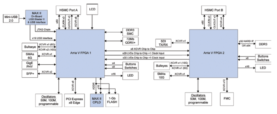
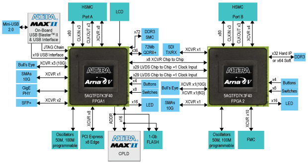
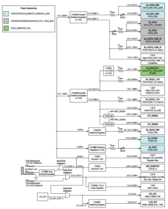
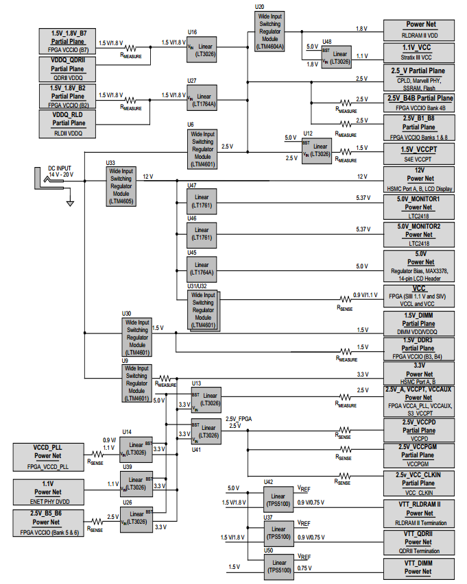
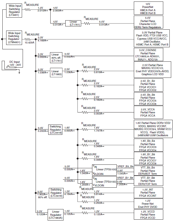
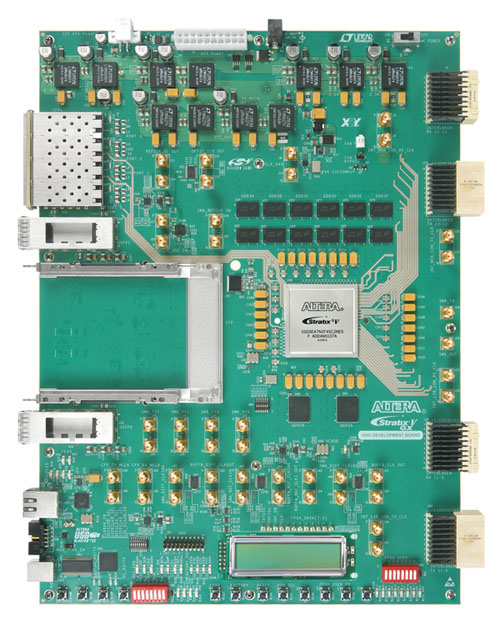
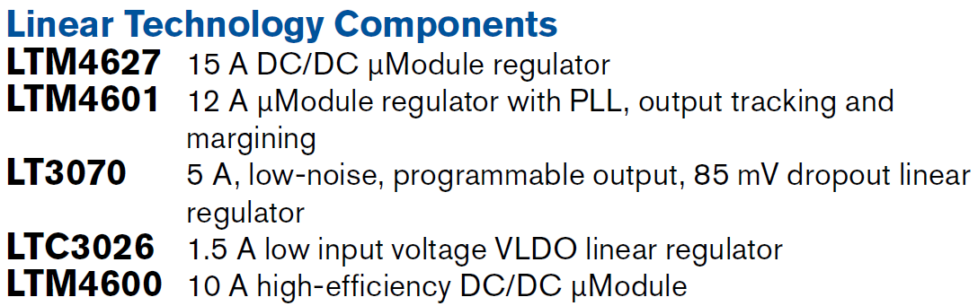
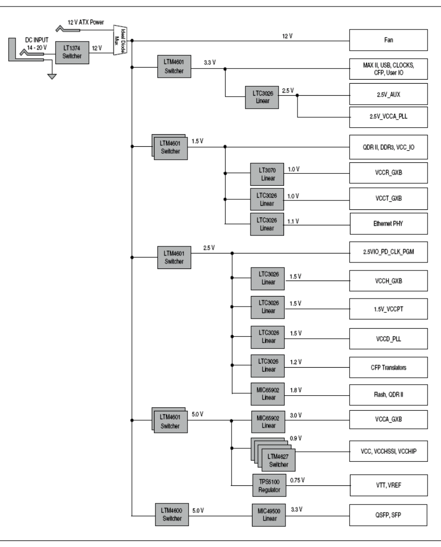
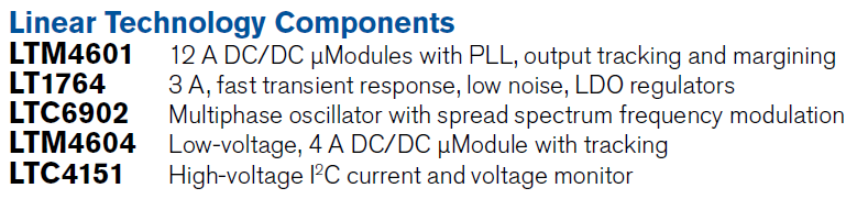
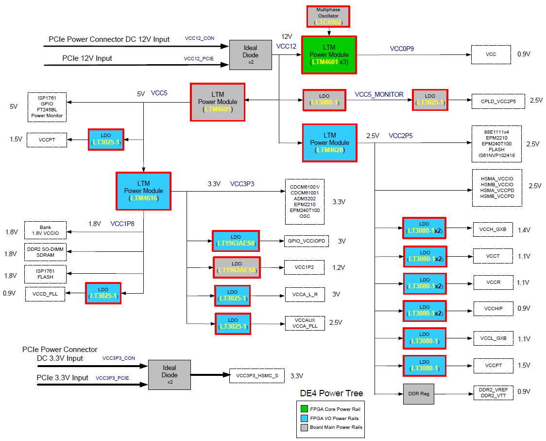
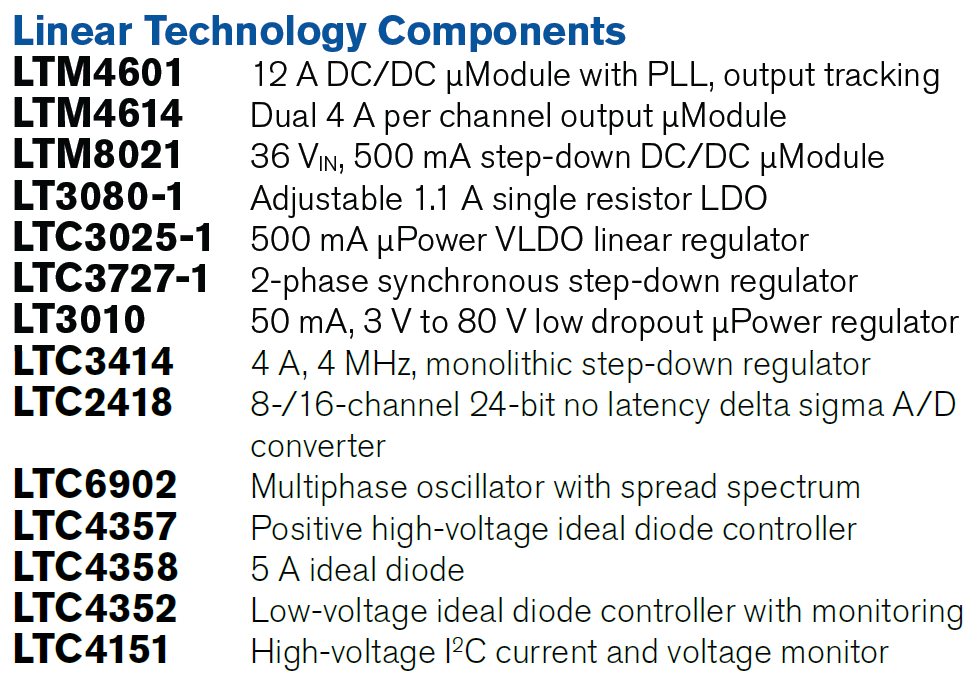
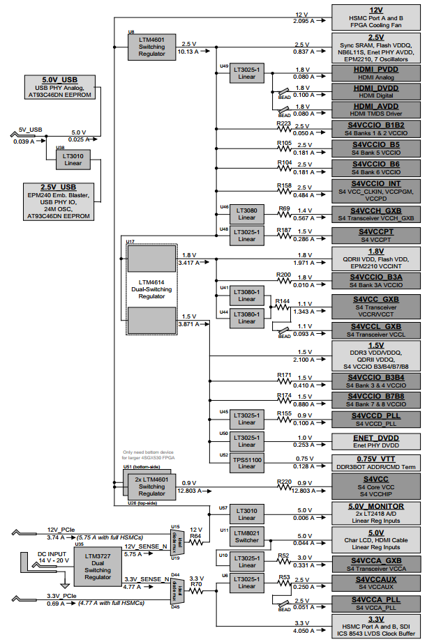
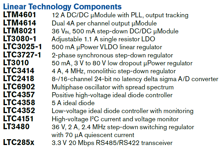
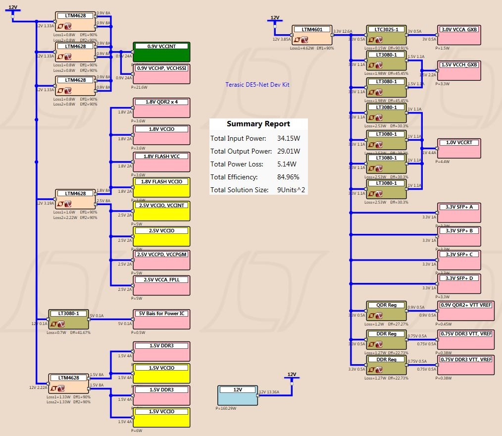
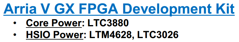
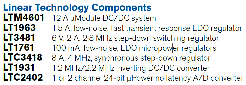
LTM4601