Interface

- Automatic Test Equipment
- Digital & Analog I/O
- Ethernet Transceivers & Switches
- Fanout Buffers & Splitters
- Flip Flops & Logic Gates
- HDMI & Video Interface
- I/O Expanders
- Interface Receivers
- Interface Transceivers & Isolators
- Interface Transmitters
- Level Translators & Buffers
- Limiting Amplifiers
- RS-232 & RS-485 Interface
- SerDes & GMSL
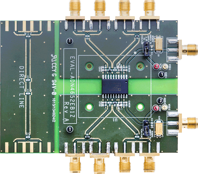
ADN4651