ADA4355
RECOMMENDED FOR NEW DESIGNSProgrammable Transimpedance, Current to Bits Receiver μModule
- Part Models
- 1
- 1ku List Price
- Starting From $126.40
Part Details
- High performance, current input, data acquisition μModule that includes a TIA, analog filter, ADC driver, and ADC
- 3 selectable TZ settings: 2 kΩ, 20 kΩ, and 200 kΩ
- Internal 1.8 V LDO for the ADC
- All passive components including supply decoupling
- Small form factor: 12.00 mm × 6.00 mm CSP_BGA
- Operation from a single 3.3 V supply
- Full-scale input current to 800 μA (TZ = 2 kΩ)
- Fast input overload recovery
- High analog input current to 40 mA
- Analog filter for noise reduction and antialias filtering
- Selectable 1.0 MHz and 100 MHz LPF bandwidth
- Low input referred current noise: 16 pA rms
- TZ = 200 kΩ, 65,536 averages, 1 MHz analog filter
- Supports input pulse widths down to 10 ns
- 14-bit ADC with sample rate up to 125 MSPS
- Serial LVDS data output
- SPI control interface
- Quiescent power: 546 mW, LDO enabled
- Temperature range: −40°C to +85°C
The ADA4355 is a complete, high performance, current input μModule®. For space savings, the ADA4355 includes all the required active and passive components to realize a complete current to bits data acquisition solution, supporting a small form factor, optical modules as well as multichannel systems.
The high speed transimpedance amplifier (TIA) of the device supports 10 ns pulse widths, allowing high spatial resolution for Time of Flight (ToF) measurements. Additionally, the ADA4355 includes three TIA gain (TZ) settings to maximize dynamic range. An internal, selectable, analog low-pass filter (LPF) can limit the device bandwidth with a corner frequency of 100 MHz to minimize broadband noise while also serving as an antialiasing filter for the 125 MSPS ADC. For lower bandwidth signals, or wider signal pulses (for example, 20 μs or wider), the filter can be set to a corner frequency of 1.0 MHz to provide additional noise reduction.
The 14-bit ADC converts the amplified voltage signal at a rate of up to 125 MSPS and outputs the digitized signals through two serial, low voltage differential signaling (LVDS) data lanes, operating at rates of up to 1 Gbps per lane. The data clock output (DCO) operates at frequencies of up to 500 MHz and supports double data rate (DDR) operation.
The ADA4355 exhibits fast overdrive recovery from a large input current signal and is available in a 12.00 mm × 6.00 mm CSP_BGA package with a −40°C to +85°C operating temperature range.
APPLICATIONS
- Current to voltage conversion
- Chemical analyzers
- Mass spectroscopy
- Time of Flight
- Fiber optic sensing
- OTDR
- Optical amplifiers
- Reconfigurable optical add and drop multiplexers (ROADM)
Documentation
Data Sheet 1
Video 7


ADI has always placed the highest emphasis on delivering products that meet the maximum levels of quality and reliability. We achieve this by incorporating quality and reliability checks in every scope of product and process design, and in the manufacturing process as well. "Zero defects" for shipped products is always our goal. View our quality and reliability program and certifications for more information.
| Part Model | Pin/Package Drawing | Documentation | CAD Symbols, Footprints, and 3D Models |
|---|---|---|---|
| ADA4355ABCZ | 84-Ball CSP-BGA (12mm x 6mm x 1.5mm) |
This is the most up-to-date revision of the Data Sheet.
Software Resources
Can't find the software or driver you need?
Request a Driver/SoftwareEvaluation Kits
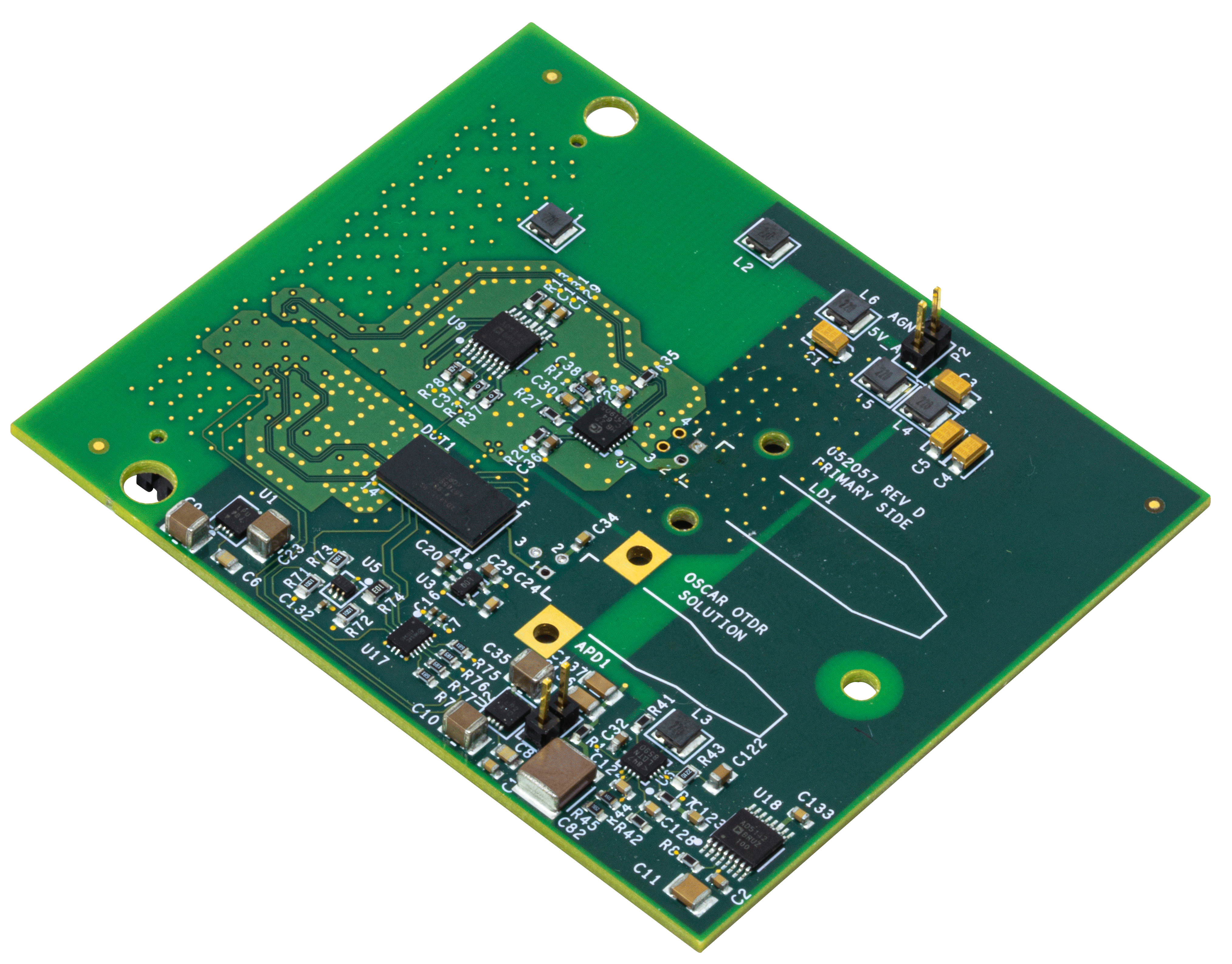
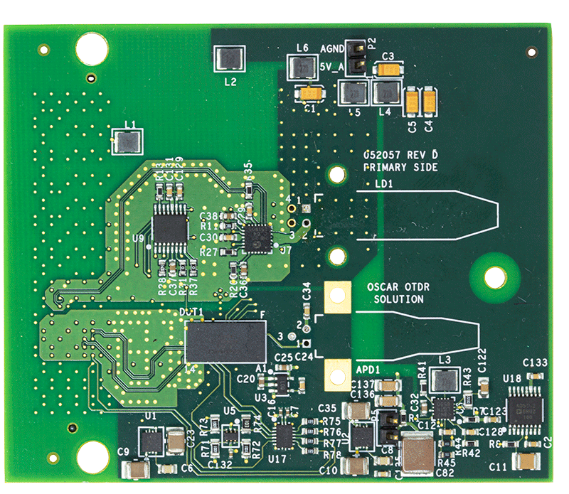
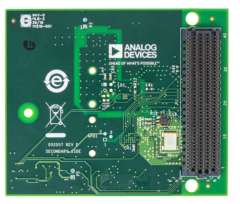
Evaluation System for the ADA4355
Resources
Latest Discussions
No discussions on ADA4355 yet. Have something to say?
Start a Discussion on EngineerZone®