
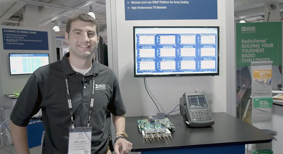
Learn the basics about RadioVerse and the technologies you can leverage in your next radio application design.
Explore ADI TransceiversAD9371
RECOMMENDED FOR NEW DESIGNSIntegrated, Dual RF Transceiver with Observation Path
- Part Models
- 2
- 1ku List Price
- Starting From $314.58
Part Details
- Dual differential transmitters (Tx)
- Dual differential receivers (Rx)
- Observation receiver (ORx) with 2 inputs
- Sniffer receiver (SnRx) with 3 inputs
- Tunable range: 300 MHz to 6000 MHz
- Tx synthesis bandwidth (BW) to 250 MHz
- Rx BW: 8 MHz to 100 MHz
- Supports frequency division duplex (FDD) and time division duplex (TDD) operation
- Fully integrated independent fractional-N radio frequency (RF) synthesizers for Tx, Rx, ORx, and clock generation
- JESD204B digital interface
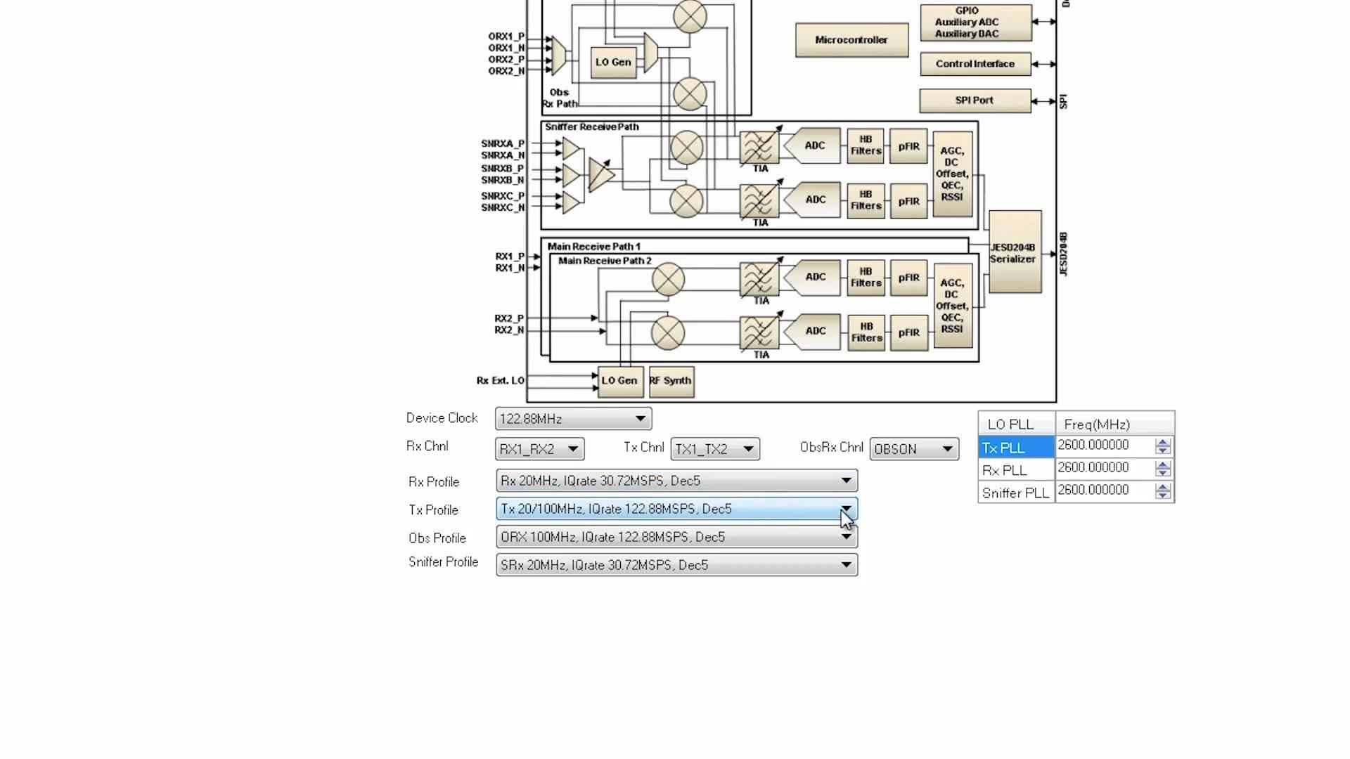
The AD9371 is a highly integrated, wideband RF transceiver offering dual channel transmitters and receivers, integrated synthesizers, and digital signal processing functions. The IC delivers a versatile combination of high performance and low power consumption required by 3G/4G micro and macro BTS equipment in both FDD and TDD applications. The AD9371 operates from 300 MHz to 6000 MHz, covering most of the licensed and unlicensed cellular bands. The IC supports receiver bandwidths up to 100 MHz. It also supports observation receiver and transmit synthesis bandwidths up to 250 MHz to accommodate digital correction algorithms.
The transceiver consists of wideband direct conversion signal paths with state-of-the-art noise figure and linearity. Each complete receiver and transmitter subsystem includes dc offset correction, quadrature error correction (QEC), and programmable digital filters, eliminating the need for these functions in the digital baseband. Several auxiliary functions such as an auxiliary analog- to-digital converter (ADC), auxiliary digital-to-analog converters (DACs), and general-purpose input/outputs (GPIOs) are integrated to provide additional monitoring and control capability.
An observation receiver channel with two inputs is included to monitor each transmitter output and implement interference mitigation and calibration applications. This channel also connects to three sniffer receiver inputs that can monitor radio activity in different bands.
The high speed JESD204B interface supports lane rates up to 6144 Mbps. Four lanes are dedicated to the transmitters and four lanes are dedicated to the receiver and observation receiver channels.
The fully integrated phase-locked loops (PLLs) provide high performance, low power fractional-N frequency synthesis for the transmitter, the receiver, the observation receiver, and the clock sections. Careful design and layout techniques provide the isolation demanded in high performance base station applications. All voltage controlled oscillator (VCO) and loop filter components are integrated to minimize the external component count.
A 1.3 V supply is required to power the core of the AD9371, and a standard 4-wire serial port controls it. Other voltage supplies provide proper digital interface levels and optimize transmitter and auxiliary converter performance. The AD9371 is packaged in a 12 mm × 12 mm, 196-ball chip scale ball grid array (CSP_BGA).
Applications
- 3G/4G micro and macro base stations (BTS)
- 3G/4G multicarrier picocells
- FDD and TDD active antenna systems
- Microwave, nonline of sight (NLOS) backhaul systems
Documentation
Data Sheet 1
User Guide 1
Application Note 1
Technical Articles 8
Product Highlight 1
Informational 1
Video 15


Solutions Bulletin & Brochure 1
Product Highlight 1
Device Drivers 2
FPGA Interoperability Reports 2
Analog Dialogue 6
Webcast 9
ADI has always placed the highest emphasis on delivering products that meet the maximum levels of quality and reliability. We achieve this by incorporating quality and reliability checks in every scope of product and process design, and in the manufacturing process as well. "Zero defects" for shipped products is always our goal. View our quality and reliability program and certifications for more information.
| Part Model | Pin/Package Drawing | Documentation | CAD Symbols, Footprints, and 3D Models |
|---|---|---|---|
| AD9371BBCZ | 196-Ball CSPBGA (12mm x 12mm x 1.27mm) | ||
| AD9371BBCZ-REEL | 196-Ball CSPBGA (12mm x 12mm x 1.27mm) |
This is the most up-to-date revision of the Data Sheet.
Software Resources
Device Drivers 2
Evaluation Software 2
Wideband RF Transceiver Evaluation Software
The Evaluation kit offers several software drivers for evaluation and rapid prototyping as well as design tool options to aid in simulation and filter design.
JESD204 Interface Framework
Integrated JESD204 software framework for rapid system-level development and optimization
Hardware Ecosystem
Tools & Simulations
MATLAB Profile Generator for AD9371
Open Tool
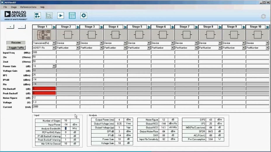
ADIsimRF
ADIsimRF is an easy-to-use RF signal chain calculator. Cascaded gain, noise, distortion and power consumption can be calculated, plotted and exported for signal chains with up to 50 stages. ADIsimRF also includes an extensive data base of device models for ADI’s RF and mixed signal components.
Open ToolSDR Integrated Transceiver Design Resources
This site contains the device documentation packages for the SDR Integrated Transceivers including user guides, IBIS models, and PCB files.
Open ToolEvaluation Kits
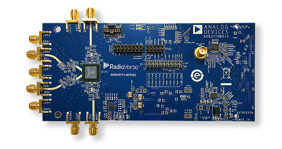

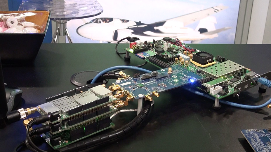
ADRV9371-N/PCBZ and ADRV9371-W/PCBZ Boards
Features and Benefits
- Complete Radio Card platform containing AD9371 with:
- 2 x Transmit outputs
- 2 x Receive inputs
- 2 x Observation inputs
- 1x Sniffer path
- Narrow tuning range and Wide tuning range options
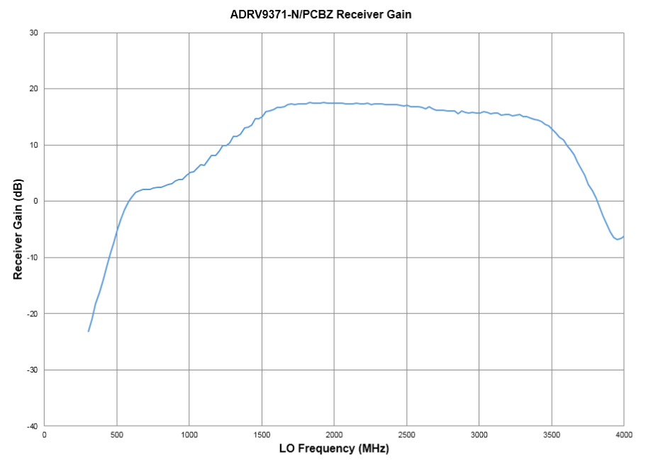
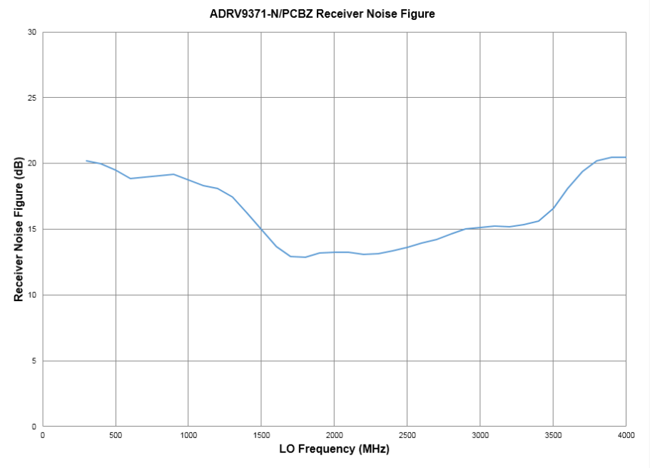
- ADRV9371-N/PCBZ matched for 1.8GHz – 2.6GHz
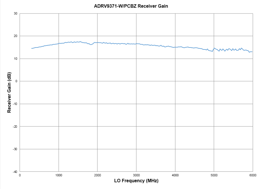
- ADRV9371-W/PCBZ matched for 300MHz – 6GHz
- Complete with high efficiency power supply solution and clocking solution for AD9371
- FMC connector to Xilinx ZC706 motherboard (EK-Z7-ZC706-G).
- Powered from single FMC connector
- Includes schematics, layout, BOM, HDL, drivers and application software
Product Details
The ADRV9371-N/PCBZ and ADRV9371-WPCBZ are radio cards designed to showcase the AD9371, a high performance wideband integrated RF transceiver intended for use in RF applications such as 4G base station, test and measurement applications and software defined radios. The radio cards provide hardware engineers, software engineers and system architects with a single 2x2 transceiver platform for device evaluation and rapid prototyping of radio solutions. All peripherals necessary for the radio card to operate including a high efficiency switcher only power supply solution, and a high performance clocking solution are populated on the board.
Both narrow tuning range and wide tuning range options exist.
The ADRV9371-N/PCBZ is optimized for performance over a narrow tuning range1.8GHz – 2.6GHz. It will exhibit diminished RF performance on tuned RF frequencies outside of this band. This board is primarily intended to provide RF engineers with the ability to connect the AD9371 to an RF test bench (Vector Signal Analyzer, Signal Generator, etc.) and achieve its optimum performance.
The ADRV9371-W/PCBZ operates over a wide tuning range 300MHz – 6GHz, however the RF performance is tempered by the very wide band front end match. This board is primarily intended for system investigation and bringing up various waveforms from a software team before custom hardware is complete. The objective being for designers to see waveforms, but not being concerned about the last 1dB or 1% EVM of performance.

The board interfaces to the Xilinx ZC706 motherboard (EK-Z7-ZC706-G) (ordered separately).
Resources
Software
Latest Discussions
No discussions on AD9371 yet. Have something to say?
Start a Discussion on EngineerZone®