AD6684
RECOMMENDED FOR NEW DESIGNS135 MHz Quad IF Receiver
- Part Models
- 2
- 1ku List Price
- Starting From $575.26
Part Details
-
JESD204B (Subclass 1) coded serial digital outputs
- Lane rates up to 15 Gbps
- 1.68 W total power at 500 MSPS
- 420 mW per analog-to-digital converter (ADC) channel
- SFDR = 82 dBFS at 305 MHz (1.8 V p-p input range)
- SNR = 66.8 dBFS at 305 MHz (1.8 V p-p input range)
- Noise density = −151.5 dBFS/Hz (1.8 V p-p input range)
- Analog input buffer
- On-chip dithering to improve small signal linearity
- Flexible differential input range
- 1.44 V p-p to 2.16 V p-p (1.80 V p-p nominal)
- 82 dB channel isolation/crosstalk
- 0.975 V, 1.8 V, and 2.5 V dc supply operation
- Noise shaping requantizer (NSR) option for main receiver
- Variable dynamic range (VDR) option for digital
- predistortion (DPD)
- 4 integrated wideband digital downconverters (DDCs)
- 48-bit numerically controlled oscillator (NCO), up to 4 cascaded half-band filters
- 1.4 GHz analog input full power bandwidth
- Amplitude detect bits for efficient automatic gain control
- (AGC) implementation
- Differential clock input
- Integer clock divide by 1, 2, 4, or 8
- On-chip temperature diode
- Flexible JESD204B lane configurations
The AD6684 is a 135 MHz bandwidth, quad intermediate frequency (IF) receiver. It consists of four 14-bit, 500 MSPS ADCs and various digital processing blocks consisting of four wideband DDCs, an NSR, and VDR monitoring. The device has an on-chip buffer and a sample-and-hold circuit designed for low power, small size, and ease of use. This device is designed to support communications applications. The analog full power bandwidth of the device is 1.4 GHz.
The quad ADC cores feature a multistage, differential pipelined architecture with integrated output error correction logic. Each ADC features wide bandwidth inputs supporting a variety of user-selectable input ranges. An integrated voltage reference eases design considerations. The AD6684 is optimized for wide input bandwidth, excellent linearity, and low power in a small package.
The analog inputs and clock signal input are differential. Each pair of ADC data outputs are internally connected to two DDCs through a crossbar mux. Each DDC consists of up to five cascaded signal processing stages: a 48-bit frequency translator, NCO, and up to four half-band decimation filters.
Each ADC output is connected internally to an NSR block. The integrated NSR circuitry allows improved SNR performance in a smaller frequency band within the Nyquist bandwidth. The device supports two different output modes selectable via the serial port interface (SPI). With the NSR feature enabled, the outputs of the ADCs are processed such that the AD6684 supports enhanced SNR performance within a limited portion of the Nyquist bandwidth while maintaining a 9-bit output resolution.
Each ADC output is also connected internally to a VDR block. This optional mode allows full dynamic range for defined input signals. Inputs that are within a defined mask (based on DPD applications) are passed unaltered. Inputs that violate this defined mask result in the reduction of the output resolution.
With VDR, the dynamic range of the observation receiver is determined by a defined input frequency mask. For signals falling within the mask, the outputs are presented at the maximum resolution allowed. For signals exceeding defined power levels within this frequency mask, the output resolution is truncated. This mask is based on DPD applications andsupports tunable real IF sampling, and zero IF or complex IF receive architectures.
Operation of the AD6684 in the DDC, NSR, and VDR modes is selectable via SPI-programmable profiles (the default mode is NSR at startup).
In addition to the DDC blocks, the AD6684 has several functions that simplify the AGC function in the communications receiver. The programmable threshold detector allows monitoring of the incoming signal power using the fast detect output bits of the ADC. If the input signal level exceeds the programmable threshold, the fast detect indicator goes high. Because this threshold indicator has low latency, the user can quickly turn down the system gain to avoid an overrange condition at the ADC input.
Users can configure each pair of IF receiver outputs onto either one or two lanes of Subclass 1 JESD204B-based high speed serialized outputs, depending on the decimation ratio and the acceptable lane rate of the receiving logic device. Multiple device synchronization is supported through the SYSREF±, SYNCINB±AB, and SYNCINB±CD input pins.
The AD6684 has flexible power-down options that allow significant power savings when desired. All of these features can be programmed using the 1.8 V capable, 3-wire SPI.
The AD6684 is available in a Pb-free, 72-lead LFCSP and is specified over the −40°C to +105°C junction temperature range.
Product Highlights
- Low power consumption per channel.
- JESD204B lane rate support up to 15 Gbps.
- Wide full power bandwidth supports IF sampling of signals up to 1.4 GHz.
- Buffered inputs ease filter design and implementation.
- Four integrated wideband decimation filters and NCO blocks supporting multiband receivers.
- Programmable fast overrange detection.
- On-chip temperature diode for system thermal management.
Applications
- Communications
- Diversity multiband, multimode digital receivers 3G/4G, W-CDMA, GSM, LTE, LTE-A
- HFC digital reverse path receivers
- Digital predistortion observation paths
- General-purpose software radios
Documentation
Data Sheet 1
User Guide 1
Application Note 1
Device Drivers 1
ADI has always placed the highest emphasis on delivering products that meet the maximum levels of quality and reliability. We achieve this by incorporating quality and reliability checks in every scope of product and process design, and in the manufacturing process as well. "Zero defects" for shipped products is always our goal. View our quality and reliability program and certifications for more information.
| Part Model | Pin/Package Drawing | Documentation | CAD Symbols, Footprints, and 3D Models |
|---|---|---|---|
| AD6684BCPZ-500 | 72-Lead LFCSP (10mm x 10mm w/ EP) | ||
| AD6684BCPZRL7-500 | 72-Lead LFCSP (10mm x 10mm w/ EP) |
This is the most up-to-date revision of the Data Sheet.
Software Resources
Device Drivers 1
Evaluation Software 1
JESD204x Frame Mapping Table Generator
The JESD204x Frame Mapping Table Generator tool consists of two Windows executables that will allow the user to input any valid combination of JESD204x parameters (L, M, F, S, NP) in order to output a .csv file that illustrates the frame mapping of the JESD204x mode in table format. There is an executable that allows the user to input a single JESD204x mode and another, that allows the user to input the parameters for multiple JESD204x modes in a specified .csv format in order to output a .csv file that illustrates the frame mapping of each of the JESD204x modes that were input into separate tables.
Can't find the software or driver you need?
Hardware Ecosystem
| Parts | Product Life Cycle | Description |
|---|---|---|
| Clocks 2 | ||
| LTC6951 | LAST TIME BUY | Ultralow Jitter Multi-Output Clock Synthesizer with Integrated VCO |
| LTC6953 | LAST TIME BUY | Ultralow Jitter, 4.5GHz Clock Distributor with 11 Outputs and JESD204B/JESD204C Support |
| Fanout Buffers & Splitters 2 | ||
| LTC6955 | LAST TIME BUY | Ultralow Jitter, 7.5GHz, 11 Output Fanout Buffer Family |
| HMC7043 | RECOMMENDED FOR NEW DESIGNS |
High Performance, 3.2 GHz, 14-Output Fanout Buffer with JESD204B/JESD204C |
| PLL Synthesizers 3 | ||
| LTC6952 | LAST TIME BUY | Ultralow Jitter, 4.5GHz PLL with 11 Outputs and JESD204B / JESD204C Support |
| HMC7044 | RECOMMENDED FOR NEW DESIGNS | High Performance, 3.2 GHz, 14-Output Jitter Attenuator with JESD204B and JESD204C Support |
| AD9528 | RECOMMENDED FOR NEW DESIGNS | JESD204B/JESD204C Clock Generator with 14 LVDS/HSTL Outputs |
Tools & Simulations
Virtual Eval - BETA
Virtual Eval is a web application to assist designers in product evaluation of ADCs, DACs, and other ADI products. Using detailed models on Analog’s servers, Virtual Eval simulates crucial part performance characteristics within seconds. Configure operating conditions such as input tones and external jitter, as well as device features like gain or digital down-conversion. Performance characteristics include noise, distortion, and resolution, FFTs, timing diagrams, response plots, and more.
Open ToolADC Companion Transport Layer RTL Code Generator Tool
This command line executable tool generates a Verilog module which implements the JESD204 receive transport layer. The user specifies in a configuration file one or more modes to be supported by the transport layer module. These modes are defined as a set of JESD204 parameter values: L, M, F, S, N', and CF. The transport layer converts JESD204 lane data output from a JESD204 link layer IP to a data bus with a fixed width, containing interleaved virtual converter samples. Both JESD204B and JESD204C link layers are supported.
Open ToolLTspice® is a powerful, fast and free simulation software, schematic capture and waveform viewer with enhancements and models for improving the simulation of analog circuits.
Evaluation Kits
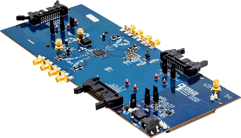
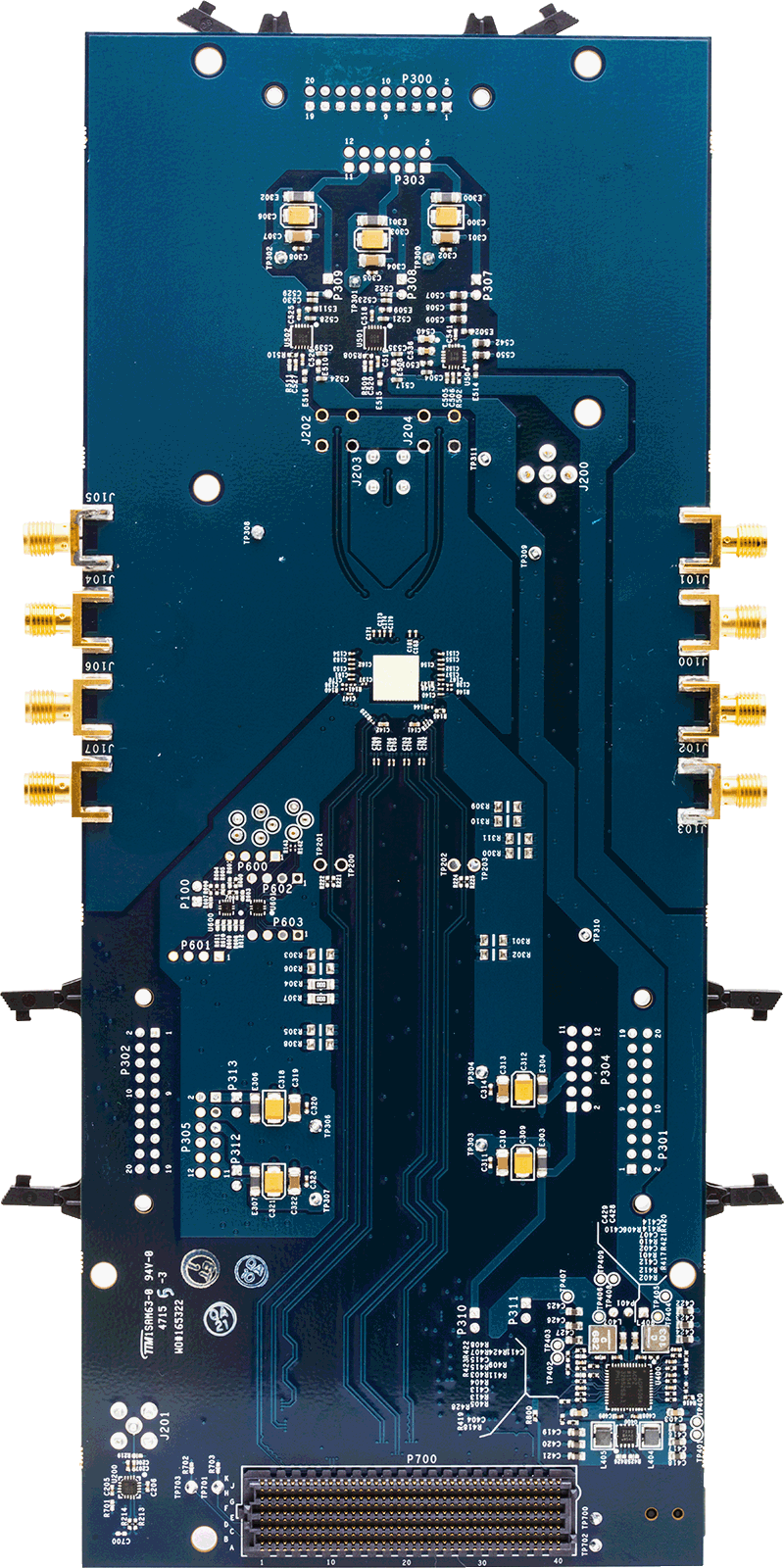
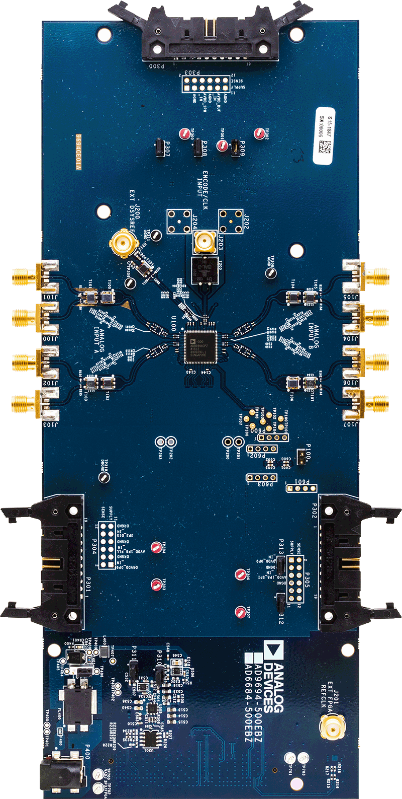
AD6684 Evaluation Board
Resources
Latest Discussions
No discussions on AD6684 yet. Have something to say?
Start a Discussion on EngineerZone®