AD6641
RECOMMENDED FOR NEW DESIGNS250 MHz Bandwidth DPD Observation Receiver
- Part Models
- 2
- 1ku List Price
- Starting From $160.44
Part Details
- SNR = 65.8 dBFS at fIN up to 250 MHz at 500 MSPS
- ENOB of 10.5 bits at fIN up to 250 MHz at 500 MSPS (−1.0 dBFS)
- SFDR = 80 dBc at fIN up to 250 MHz at 500 MSPS (−1.0 dBFS)
- Excellent linearity
- DNL = ±0.5 LSB typical, INL = ±0.6 LSB typical
- Integrated 16k × 12 FIFO
- FIFO readback options
- 12-bit parallel CMOS at 62.5 MHz
- 6-bit DDR LVDS interface
- SPORT at 62.5 MHz
- SPI at 25 MHz
- High speed synchronization capability
- 1 GHz full power analog bandwidth
- Integrated input buffer
- On-chip reference, no external decoupling required
- Low power dissipation
- 695 mW at 500 MSPS
- Programmable input voltage range
- 1.18 V to 1.6 V, 1.5 V nominal
- 1.9 V analog and digital supply operation
- 1.9 V or 3.3 V SPI and SPORT operation
- Clock duty cycle stabilizer
- Integrated data clock output with programmable clock and data alignment
The AD6641 is a 250 MHz bandwidth digital predistortion (DPD) observation receiver that integrates a 12-bit 500 MSPS ADC, a 16k × 12 FIFO, and a multimode back end that allows users to retrieve the data through a serial port (SPORT), the SPI interface, a 12-bit parallel CMOS port, or a 6-bit DDR LVDS port after being stored in the integrated FIFO memory. It is optimized for outstanding dynamic performance and low power consumption and is suitable for use in telecommunications applications such as a digital predistortion observation path where wider bandwidths are desired. All necessary functions, including the sample-and-hold and voltage reference, are included on the chip to provide a complete signal conversion solution.
The on-chip FIFO allows small snapshots of time to be captured via the ADC and read back at a lower rate. This reduces the constraints of signal processing by transferring the captured data at an arbitrary time and at a much lower sample rate. The FIFO can be operated in several user-programmable modes. In the single capture mode, the ADC data is captured when signaled via the SPI port or the use of the external FILL± pins. In the continuous capture mode, the data is loaded continuously into the FIFO and the FILL± pins are used to stop this operation.
The data stored in the FIFO can be read back based on several user-selectable output modes. The DUMP pin can be asserted to output the FIFO data. The data stored in the FIFO can be accessed via a SPORT, SPI, 12-bit parallel CMOS port, or 6-bit DDR LVDS interface. The maximum output throughput supported by the AD6641 is in the 12-bit CMOS or 6-bit DDR LVDS mode and is internally limited to 1/8th of the maximum input sample rate. This corresponds to the maximum output data rate of 62.5 MHz at an input clock rate of 500 MSPS.
The ADC requires a 1.9 V analog voltage supply and a differential clock for full performance operation. Output format options include twos complement, offset binary format, or Gray code. A data clock output is available for proper output data timing. Fabricated on an advanced SiGe BiCMOS process, the device is available in a 56-lead LFCSP and is specified over the industrial temperature range (−40°C to +85°C). This product is protected by a U.S. patent.
Applications
- Wireless and wired broadband communications
- Communications test equipment
- Power amplifier linearization
Product Highlights
- High Performance ADC Core.
Maintains 65.8 dBFS SNR at 500 MSPS with a 250 MHz input. - Low Power. Consumes only 695 mW at 500 MSPS.
- Ease of Use.
On-chip 16k FIFO allows the user to target the high performance ADC to the time period of interest and reduce the constraints of processing the data by transferring it at an arbitrary time and a lower sample rate. The on-chip reference and sample-and-hold provide flexibility in system design. Use of a single 1.9 V supply simplifies system power supply design. - Serial Port Control.
Standard serial port interface supports configuration of the device and customization for the user’s needs. - 1.9 V or 3.3 V SPI and Serial Data Port Operation.
Documentation
Data Sheet 1
User Guide 1
Application Note 12
Technical Articles 1
ADI has always placed the highest emphasis on delivering products that meet the maximum levels of quality and reliability. We achieve this by incorporating quality and reliability checks in every scope of product and process design, and in the manufacturing process as well. "Zero defects" for shipped products is always our goal. View our quality and reliability program and certifications for more information.
| Part Model | Pin/Package Drawing | Documentation | CAD Symbols, Footprints, and 3D Models |
|---|---|---|---|
| AD6641BCPZ-500 | 56 ld LFCSP (8x8mm) | ||
| AD6641BCPZRL7-500 | 56 ld LFCSP (8x8mm) |
| Part Models | Product Lifecycle | PCN |
|---|---|---|
|
Jun 9, 2021 - 20_0126 Conversion of Select Sizes LFCSP Products from Punched to Sawn and Transfer of Assembly Site to ASE Korea |
||
| AD6641BCPZ-500 | PRODUCTION | |
| AD6641BCPZRL7-500 | PRODUCTION | |
This is the most up-to-date revision of the Data Sheet.
Software Resources
Can't find the software or driver you need?
Request a Driver/SoftwareHardware Ecosystem
| Parts | Product Life Cycle | Description |
|---|---|---|
| Clock ICs 8 | ||
| AD9510 | RECOMMENDED FOR NEW DESIGNS | 1.2 GHz Clock Distribution IC, PLL Core, Dividers, Delay Adjust, Eight Outputs |
| AD9511 | RECOMMENDED FOR NEW DESIGNS | 1.2 GHz Clock Distribution IC, PLL Core, Dividers, Delay Adjust, Five Outputs |
| AD9512 | RECOMMENDED FOR NEW DESIGNS | 1.2 GHz Clock Distribution IC, Two 1.6 GHz Inputs, Dividers, Delay Adjust, Five Outputs |
| AD9513 | RECOMMENDED FOR NEW DESIGNS | 800 MHz Clock Distribution IC, Dividers, Delay Adjust, Three Outputs |
| AD9514 | RECOMMENDED FOR NEW DESIGNS | 1.6 GHz Clock Distribution IC, Dividers, Delay Adjust, Three Outputs |
| AD9515 | RECOMMENDED FOR NEW DESIGNS | 1.6 GHz Clock Distribution IC, Dividers, Delay Adjust, Two Outputs |
| AD9523 | NOT RECOMMENDED FOR NEW DESIGNS | 14-Output, Low Jitter Clock generator |
| AD9524 | NOT RECOMMENDED FOR NEW DESIGNS | 6 Output, Dual Loop Clock Generator |
| Differential Amplifiers 3 | ||
| ADA4927-2 | RECOMMENDED FOR NEW DESIGNS | Ultralow Distortion Current Feedback Differential ADC Driver |
| ADA4938-2 | RECOMMENDED FOR NEW DESIGNS | Ultralow Distortion Differential ADC Driver (Dual) |
| ADL5562 | RECOMMENDED FOR NEW DESIGNS | 3.3 GHz Ultralow Distortion RF/IF Differential Amplifier |
| RF Amplifiers 1 | ||
| ADL5202 | Obsolete | Wide Dynamic Range, High Speed, Digitally Controlled VGA |
| RF VGAs (Variable Gain Amplifiers) 1 | ||
| AD8376 | RECOMMENDED FOR NEW DESIGNS | Ultralow Distortion IF Dual VGA |
Tools & Simulations
AD6641 IBIS Model 1
Visual Analog
For designers who are selecting or evaluating high speed ADCs, VisualAnalog™ is a software package that combines a powerful set of simulation and data analysis tools with a user-friendly graphical interface.
Open ToolEvaluation Kits
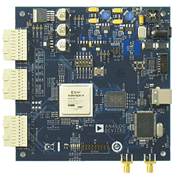
AD6641 Evaluation Board
Resources
FPGA-Based Data Capture Kit
Resources
Software
Latest Discussions
No discussions on AD6641 yet. Have something to say?
Start a Discussion on EngineerZone®