ADRV9026
RECOMMENDED FOR NEW DESIGNSIntegrated, Quad RF Transceiver with Observation Path
- Part Models
- 2
- 1ku List Price
- Starting From $885.96
Part Details
- 4 differential transmitters
- 4 differential receivers
- 2 observation receivers with 2 inputs each
- Center frequency: 75 MHz to 6000 MHz
- Maximum receiver bandwidth: 200 MHz
- Maximum transmitter large signal bandwidth: 200 MHz
- Maximum transmitter synthesis bandwidth: 450 MHz
- Maximum observation receiver bandwidth: 450 MHz
- Fully integrated independent fractional-N radio frequency synthesizers
- Fully integrated clock synthesizer
- Multichip phase synchronization for all local oscillators and baseband clocks
- Support for TDD and FDD applications
- 24.33 Gbps JESD204B/JESD204C digital interface
The ADRV9026 is a highly integrated, radio frequency (RF) agile transceiver offering four independently controlled transmitters, dedicated observation receiver inputs for monitoring each transmitter channel, four independently controlled receivers, integrated synthesizers, and digital signal processing functions providing a complete transceiver solution. The device provides the performance demanded by cellular infrastructure applications, such as small cell base station radios, macro 3G/4G/5G systems, and massive multiple in/multiple out (MIMO) base stations.
The receiver subsystem consists of four independent, wide bandwidth, direct conversion receivers with wide dynamic range. The four independent transmitters use a direct conversion modulator resulting in low noise operation with low power consumption. The device also includes two wide bandwidth, time shared, observation path receivers with two inputs each for monitoring transmitter outputs.
The complete transceiver subsystem includes automatic and manual attenuation control, dc offset correction, quadrature error correction (QEC), and digital filtering, eliminating the need for these functions in the digital baseband. Other auxiliary functions such as analog-to-digital converters (ADCs), digital-to-analog converters (DACs), and general-purpose input/outputs (GPIOs) that provide an array of digital control options are also integrated.
To achieve a high level of RF performance, the transceiver includes five fully integrated phase-locked loops (PLLs). Two PLLs provide low noise and low power fractional-N RF synthesis for the transmitter and receiver signal paths. A third fully integrated PLL supports an independent local oscillator (LO) mode for the observation receiver. The fourth PLL generates the clocks needed for the converters and digital circuits, and a fifth PLL provides the clock for the serial data interface.
A multichip synchronization mechanism synchronizes the phase of all LOs and baseband clocks between multiple ADRV9026 chips. All voltage controlled oscillators (VCOs) and loop filter components are integrated and adjustable through the digital control interface.
The serial data interface consists of four serializer lanes and four deserializer lanes. The interface supports both the JESD204B and JESD204C standards, operating at data rates up to 24.33 Gbps. The interface also supports interleaved mode for lower bandwidths, thus reducing the number of high speed data interface lanes to one. Both fixed and floating-point data formats are supported. The floating-point format allows internal automatic gain control (AGC) to be invisible to the demodulator device.
The ADRV9026 is powered directly from 1.0 V, 1.3 V, and 1.8 V regulators and is controlled via a standard serial peripheral interface (SPI) serial port. Comprehensive power-down modes are included to minimize power consumption in normal use. The ADRV9026 is packaged in a 14 mm × 14 mm, 289-ball chip scale ball grid array (CSP_BGA).
Applications
- 3G/4G/5G TDD and FDD massive MIMO, macro and small cell base stations
Getting Started
Please visit the ADRV9026 landing page to download the Design File Package and the Software Package. The Design File Package includes the eval board schematics, BOM, layout, IBIS, BSDL models, JCOM models, Material Declaration, and Symbols and Footprints. The Software Package includes the GUI software, the API source code, the firmware, and the gain tables.
Documentation
Data Sheet 1
User Guide 3
Technical Articles 3
Product Highlight 1
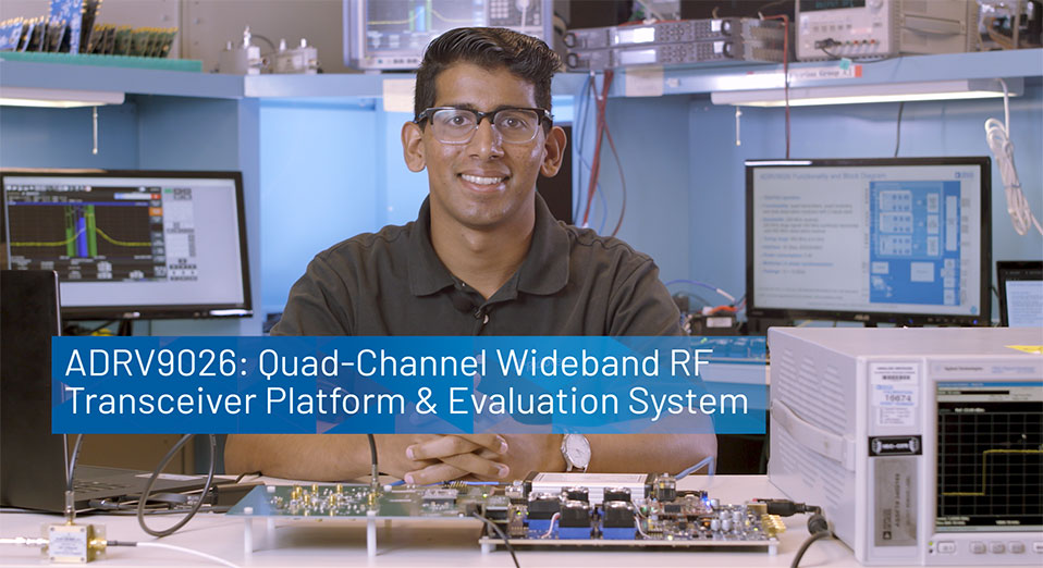
Video 1
Device Drivers 1
Solutions Bulletin & Brochure 1
Product Selection Guide 1
Product Highlight 1
Analog Dialogue 1
Thought Leadership Page 2
Webcast 1
ADI has always placed the highest emphasis on delivering products that meet the maximum levels of quality and reliability. We achieve this by incorporating quality and reliability checks in every scope of product and process design, and in the manufacturing process as well. "Zero defects" for shipped products is always our goal. View our quality and reliability program and certifications for more information.
| Part Model | Pin/Package Drawing | Documentation | CAD Symbols, Footprints, and 3D Models |
|---|---|---|---|
| ADRV9026BBCZ | 289-Ball CSPBGA (14mm x 14mm x 1.34mm) | ||
| ADRV9026BBCZ-REEL | 289-Ball CSPBGA (14mm x 14mm x 1.34mm) |
| Part Models | Product Lifecycle | PCN |
|---|---|---|
| No Match Found | ||
|
Nov 30, 2020 - 20_0305 Minor Silicon and Package Laminate Changes to ADRV9026 |
||
| ADRV9026BBCZ | PRODUCTION | |
| ADRV9026BBCZ-REEL | ||
This is the most up-to-date revision of the Data Sheet.
Software Resources
Device Drivers 1
Evaluation Software 3
ADRV9026/ADRV9029 - SDCARD
The ADRV9026-SDCARD included with the evaluation kit was up to date at the time of packaging the kit. If an update is necessary, the user will be prompted to update the image when connecting to the GUI. If the card does not function properly or users would like to create their own SD card, this image file can be downloaded and used to write a new card or overwrite the ADRV9026-SDCARD included with the evaluation kit. To program a card using this image, follow the programming instructions after downloading the image to a local drive. Note that a 16 GB minimum SD card is required when programming a new card.
ADRV9026/ADRV9029 Release Build Software Release Notes SW6.4.0.19
The SW6.4.0.19 RELEASE build provides updates in the ARM firmware, stream files, API, and GUI software to support ADRV9026/ADRV9029.
ADRV9026 Released Software SW6.4.0.19
The ADRV9026 software package contains the GUI software, the API source code, the firmware file, and the gain tables. The GUI software enables transceiver testing using the evaluation board and the Windows GUI. The API source code is intended for use in a customer system and can be integrated with the rest of the customer code and compiled for the target system. The firmware file in binary format is used by the ARM® processor on the transceivers. The gain tables include the receiver gain tables and transmitter attenuation table. Note that the files within the zip must be used together. For example, the ARM files from one zip file cannot be used with the API files from another version.
Tools & Simulations
Design Tool 1
ADIsimRF
ADIsimRF is an easy-to-use RF signal chain calculator. Cascaded gain, noise, distortion and power consumption can be calculated, plotted and exported for signal chains with up to 50 stages. ADIsimRF also includes an extensive data base of device models for ADI’s RF and mixed signal components.
Open ToolEvaluation Kits
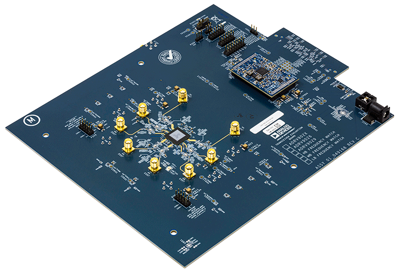
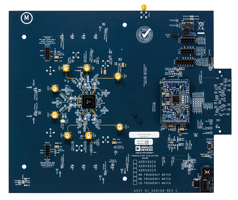
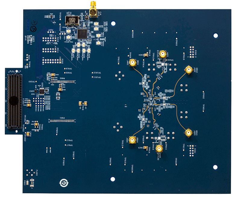
ADRV9026 and ADRV9029 Evaluation Board
Resources
Software
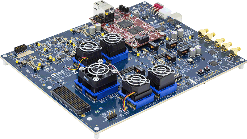
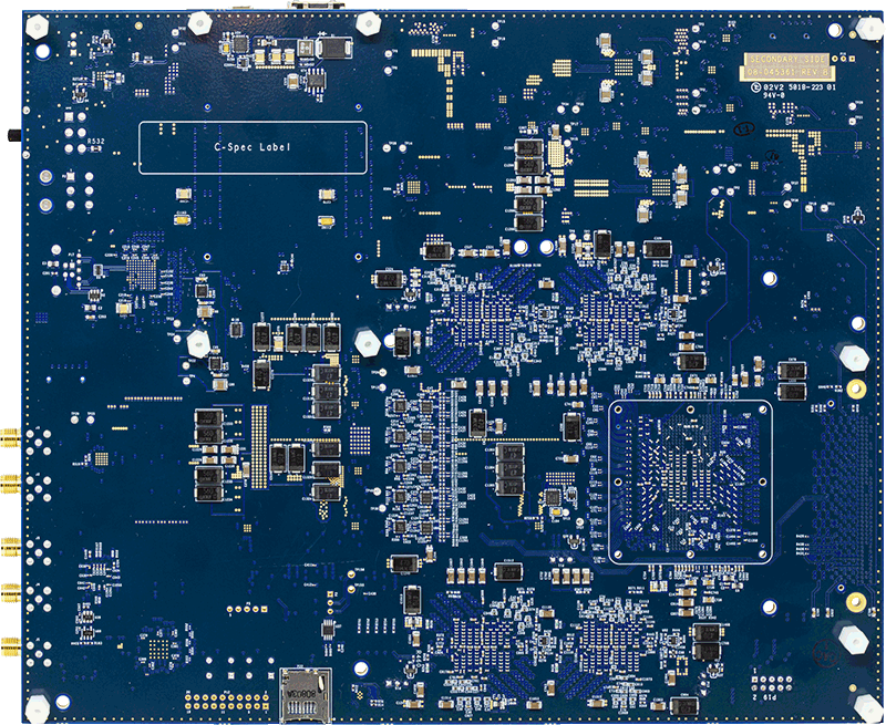
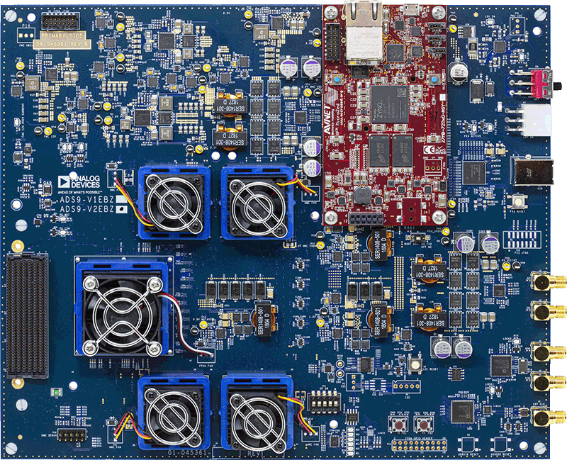
ADS9-V2EBZ Evaluation Board
Resources
Latest Discussions
No discussions on ADRV9026 yet. Have something to say?
Start a Discussion on EngineerZone®