
RadioVerse has the tools, reference designs, modules, and support for 5G and other advanced radio applications.
Explore RadioVerse solutionsADRV9009
RECOMMENDED FOR NEW DESIGNSIntegrated Dual RF Tx, Rx, and Observation Rx
- Part Models
- 2
- 1ku List Price
- Starting From $409.60
Part Details
- Dual transmitters
- Dual receivers
- Dual input shared observation receiver
- Maximum receiver bandwidth: 200 MHz
- Maximum tunable transmitter synthesis bandwidth: 450 MHz
- Maximum observation receiver bandwidth: 450 MHz
- Fully integrated fractional-N RF synthesizers
- Fully integrated clock synthesizer
- Multichip phase synchronization for RF LO and baseband clocks
- JESD204B datapath interface
- Tuning range (center frequency): 75 MHz to 6000 MHz
The ADRV9009 is a highly integrated, radio frequency (RF), agile transceiver offering dual transmitters and receivers, integrated synthesizers, and digital signal processing functions. The IC delivers a versatile combination of high performance and low power consumption demanded by 3G, 4G, and 5G macro cell time division duplex (TDD) base station applications.
The receive path consists of two independent, wide bandwidth, direct conversion receivers with state-of-the-art dynamic range. The device also supports a wide bandwidth, time shared observation path receiver (ORx) for use in TDD applications. The complete receive subsystem includes automatic and manual attenuation control, dc offset correction, quadrature error correction (QEC), and digital filtering, thus eliminating the need for these functions in the digital baseband. Several auxiliary functions, such as analog-to-digital converters (ADCs), digital-to-analog converters (DACs), and general-purpose inputs/outputs (GPIOs) for the power amplifier (PA), and RF front-end control are also integrated.
In addition to automatic gain control (AGC), the ADRV9009 also features flexible external gain control modes, allowing significant flexibility in setting system level gain dynamically.
The received signals are digitized with a set of four high dynamic range, continuous time Σ-Δ ADCs that provide inherent antialiasing. The combination of the direct conversion architecture, which does not suffer from out of band image mixing, and the lack of aliasing, relaxes the requirements of the RF filters when compared to traditional intermediate frequency (IF) receivers.
The transmitters use an innovative direct conversion modulator that achieves high modulation accuracy with exceptionally low noise.
The observation receiver path consists of a wide bandwidth, direct conversion receiver with state-of-the-art dynamic range.
The fully integrated phase-locked loop (PLL) provides high performance, low power, fractional-N RF frequency synthesis for the transmitter (Tx) and receiver (Rx) signal paths. An additional synthesizer generates the clocks needed for the converters, digital circuits, and the serial interface. A multichip synchronization mechanism synchronizes the phase of the RF local oscillator (LO) and baseband clocks between multiple ADRV9009 chips. Precautions are taken to provide the isolation required in high performance base station applications. All voltage controlled oscillators (VCOs) and loop filter components are integrated.
The high speed JESD204B interface supports up to 12.288 Gbps lane rates, resulting in two lanes per transmitter and a single lane per receiver in the widest bandwidth mode. The interface also supports interleaved mode for lower bandwidths, thus reducing the total number of high speed data interface lanes to one. Both fixed and floating point data formats are supported. The floating point format allows internal AGC to be invisible to the demodulator device.
The core of the ADRV9009 can be powered directly from 1.3 V regulators and 1.8 V regulators, and is controlled via a standard 4-wire serial port. Comprehensive power-down modes are included to minimize power consumption in normal use. The ADRV9009 is packaged in a 12 mm × 12 mm, 196-ball chip scale ball grid array (CSP_BGA).
Applications
- 3G, 4G, and 5G TDD macrocell base stations
- TDD active antenna systems
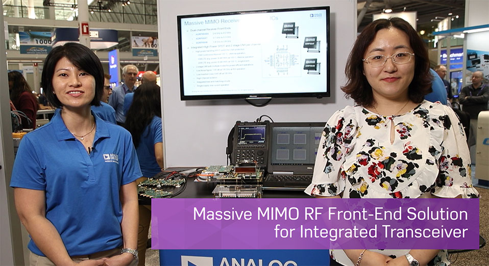
- Massive multiple input, multiple output (MIMO)
- Phased array radar
- Electronic warfare
- Military communications
- Portable test equipment
Documentation
Data Sheet 1
User Guide 1
Design Note 1
Technical Articles 10
Video 12


Device Drivers 2
Solutions Bulletin & Brochure 1
Product Selection Guide 1
Analog Dialogue 2
Webcast 6
ADI has always placed the highest emphasis on delivering products that meet the maximum levels of quality and reliability. We achieve this by incorporating quality and reliability checks in every scope of product and process design, and in the manufacturing process as well. "Zero defects" for shipped products is always our goal. View our quality and reliability program and certifications for more information.
| Part Model | Pin/Package Drawing | Documentation | CAD Symbols, Footprints, and 3D Models |
|---|---|---|---|
| ADRV9009BBCZ | 196-Ball CSPBGA (12mm x 12mm) | ||
| ADRV9009BBCZ-REEL | 196-Ball CSPBGA (12mm x 12mm) |
This is the most up-to-date revision of the Data Sheet.
Software Resources
Device Drivers 2
Evaluation Software 1
Wideband RF Transceiver Evaluation Software
The Evaluation kit offers several software drivers for evaluation and rapid prototyping as well as design tool options to aid in simulation and filter design.
Tools & Simulations
ADIsimRF
ADIsimRF is an easy-to-use RF signal chain calculator. Cascaded gain, noise, distortion and power consumption can be calculated, plotted and exported for signal chains with up to 50 stages. ADIsimRF also includes an extensive data base of device models for ADI’s RF and mixed signal components.
Open ToolSDR Integrated Transceiver Design Resources
This site contains the device documentation packages for the SDR Integrated Transceivers including user guides, IBIS models, and PCB files.
Open ToolEvaluation Kits


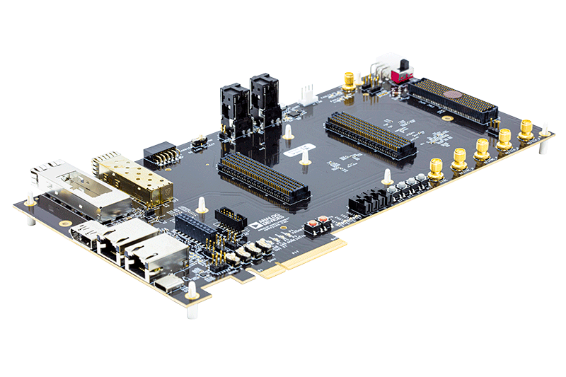
RF System on Module using the ADRV9009 Wideband Transceiver
Resources
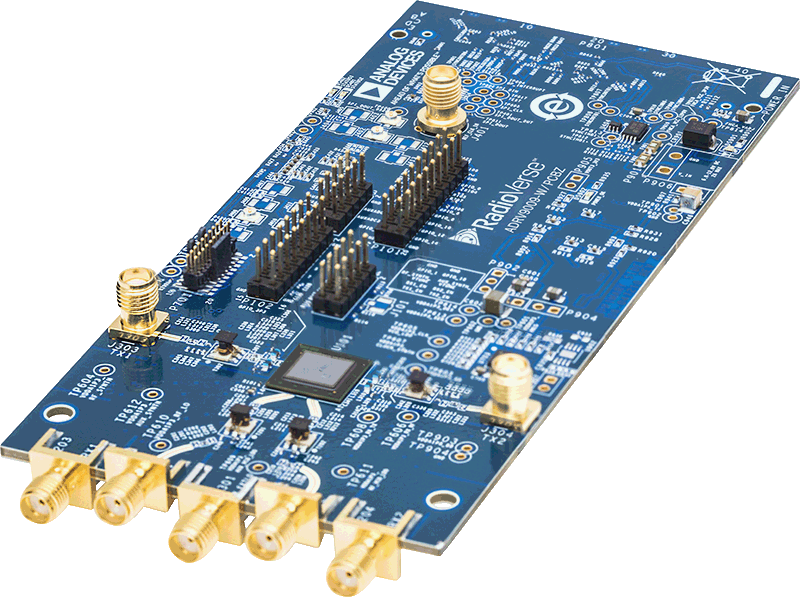

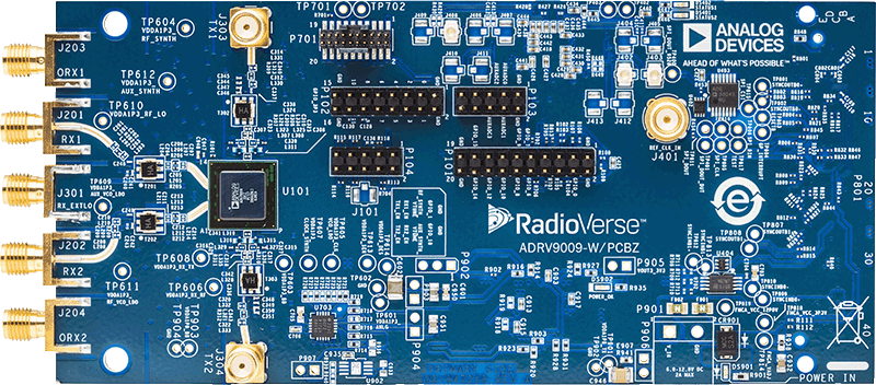
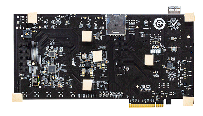
ADRV9008/ADRV9009 Evaluation Board
Resources
Software


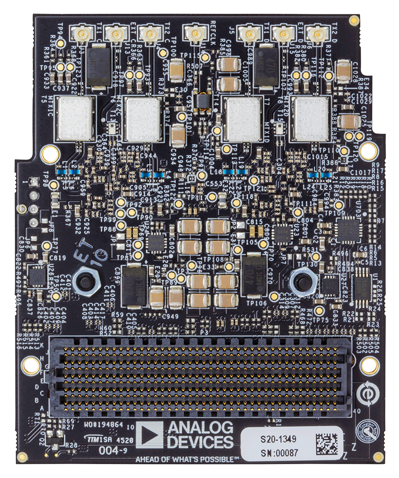
Dual ADRV9009 FMC Compatible Prototyping Platform
Resources
Software
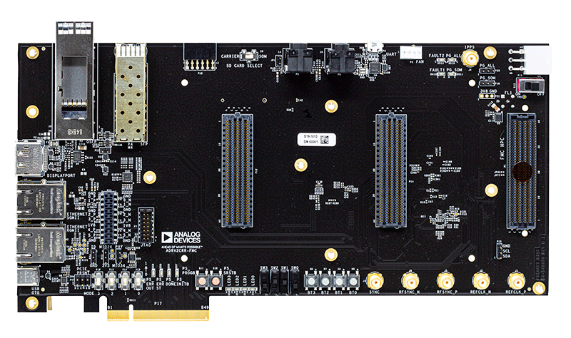
ADRV9009-ZU11EG Evaluation Carrier Board
Resources
Latest Discussions
No discussions on ADRV9009 yet. Have something to say?
Start a Discussion on EngineerZone®