ADAQ7768-1
RECOMMENDED FOR NEW DESIGNS24-Bit Single Channel Precision μModule Data Acquisition System
- Part Models
- 1
- 1ku List Price
- Starting From $21.78
Part Details
- Highly-integrated data acquisition solution
- Seven programmable-gain options
- G = 0.325, 0.65, 1.3, 2.6, 5.2, 10.4, 20.8 V/V
- Maximum input range of ±12.6 V differential
- Maximum input common-mode range of -12 V to +12 V
- Fourth-order AAF with maximum flatness and linear phase
- Full aliasing protection with 100 dB typical rejection
- Excellent device-to-device phase matching and drift
- Combined precision AC and DC performance:
- Total system dynamic range up to 130 dB
- −120 dB typical THD at 0.325 V/V gain
- 100 dB minimum DC CMRR at 20.8 V/V gain
- 25 pA maximum input bias current at 25°C
- ±6 ppm typical INL
- 5.5 ppm/°C maximum gain error drift
- ±0.13° maximum device-to-device phase mismatch at 20 kHz
- Programmable output data rate, filter type, and latency
- Linear phase digital filter options:
- Wideband low-ripple FIR filter (110 kHz maximum input bandwidth)
- Sinc5 filter (1.024 MSPS, 198.4 kHz maximum input bandwidth, 4 μs maximum group delay)
- Sinc3 filter (50 Hz/60 Hz rejection)
- Integrated LDO
- Built-in supply decoupling capacitors
- Configuration through pin strapping or SPI
- Digital interface optimized for isolated applications
- Suite of diagnostic check mechanisms
- Operating temperature range: −40°C to +85°C
- Packaging: 12.00 mm × 6.00 mm 84-ball CSP_BGA with an 0.80 mm ball pitch
- 10× footprint reduction vs. discrete solution
The ADAQ7768-1 is a 24-bit precision data acquisition (DAQ) μModule® system that encapsulates signal conditioning, conversion, and processing blocks into one system-in-package (SiP) design for the rapid development of highly compact, high-performance precision DAQ systems.
The ADAQ7768-1 consists of:
- A low-noise, low-bias current, high-bandwidth programmablegain instrumentation amplifier (PGIA) also capable of signal amplification and signal attenuation while maintaining high input impedance.
- A fourth-order, low-noise, linear phase anti-aliasing filter.
- A low-noise, low-distortion, high-bandwidth ADC driver plus an optional linearity boost buffer.
- A high-performance medium bandwidth 24-bit Σ-Δ ADC with programmable digital filter.
- A low-noise, low-dropout linear regulator.
- Reference buffers.
- Critical passive components required for the signal chain.
The ADAQ7768-1 supports fully differential input signal with a maximum range of ±12.6 V. It has an input common-mode voltage range of ±12 V with excellent common-mode rejection ratio (CMRR).
The input signal is fully buffered with very low input bias current of 2 pA typical. This allows easy input impedance matching and enables the ADAQ7768-1 to directly interface to sensors with high output impedance.
The seven pin-configurable gain settings offer additional system dynamic range and improved signal chain noise performance with input signals of lower amplitude.
A fourth-order low-pass analog filter combined with the user-programmable digital filter ensures the signal chain is fully protected against the high frequency noise and out-of-band tones presented at the input node from aliasing back into the band of interest. The analog low-pass filter is carefully designed to achieve high phase linearity and maximum in-band magnitude response flatness. Constructed with Analog Devices’s iPASSIVES™ technology, the resistor network used within the analog low-pass filter possesses superior resistance matching in both absolute values and overtemperature. As a result, the signal chain performance is maintained with minimum drift overtemperature and the ADAQ7768-1 has a tight phase mismatch across devices.
A high-performance ADC driver amplifier ensures the full settling of the ADC input at the maximum sampling rate. The driver circuit is designed for minimum additive noise, error, and distortion while maintaining stability. The fully differential architecture helps to maximize the signal chain dynamic range.
The analog-to-digital converter (ADC) inside the ADAQ7768-1 is a high-performance, 24-bit precision, single-channel sigma-delta converter with excellent AC performance and DC precision, and the throughput rate of 256 kSPS from a 16.384 MHz MCLK.
An optional linearity boost buffer further improves the signal chain linearity.
The ADAQ7768-1 is specified with the input reference voltage of 4.096 V, but the device can support reference voltages ranging from VDD_ADC down to 1 V.
The ADAQ7768-1 has two types of reference buffers: a precharge reference buffer to ease the reference input driving requirement or a full reference buffer to provide high impedance reference input. Both buffers are optional and can be turned off through register configuration.
ADAQ7768-1 supports three clock input types: crystal, complementary- metal-oxide-semiconductor (CMOS), or low-voltage differential signaling (LVDS).
Three types of digital low pass filters are available on the ADAQ7768-1. The wideband filter offers a filter profile similar to an ideal brick wall filter, making it ideal for frequency analysis. The sinc5 filter offers a low latency path with a smooth step response while maintaining a good level of aliasing rejection. It also supports an output data rate up to 1.024 MSPS from a 16.384 MHz MCLK, making the sinc5 filter ideal for low latency data capturing and time domain analysis. The sinc3 filter supports a wide decimation ratio and can produce output data rate down to 50 SPS from a 16.384 MHz MCLK. This, combined with the simultaneous 50Hz/ 60Hz rejection post filter, makes the sinc3 filter especially useful for precision DC measurement. All the three digital filters on the ADAQ7768-1 are FIR filters with linear phase response. The bandwidths of the filters, which directly correspond to the bandwidth of the DAQ signal chain, are fully programmable through register configuration.
The ADAQ7768-1 also supports two device configuration methods. The user has the option to choose to configure the device through register write through its SPI, or through a simple hardware pin strapping method to configure the device to operate under a number of predefined modes.
A single SPI supports both the register access and sample data readback functions. The ADAQ7768-1 always acts as a SPI target. Multiple interface modes are supported with a minimum of three IO channels required to communicate with the device.
The ADAQ7768-1 also features a suite of internal diagnostic functions to detect a broad range of errors during operation to improve the system reliability.
The ADAQ7768-1 device has an operating temperature range of −40°C to +85°C and is available in a 12.00 mm × 6.00 mm 84-ball CSP_BGA package with an 0.80 mm ball pitch, which makes it ideal for multiple channel applications. The ADAQ7768-1 uses only 75 mm2 of board space, 10 times less than the discrete solution that uses 750 mm2.
APPLICATIONS
- Universal input measurement platform
- Electrical test and measurement
- Sound and vibration, acoustic and material science research and development
- Control and hardware in loop verification
- Condition monitoring for predictive maintenance
- Audio test
Documentation
Data Sheet 1
User Guide 1
Video 3


3rd Party Solutions 1
Analog Dialogue 2
Webcast 3
ADI has always placed the highest emphasis on delivering products that meet the maximum levels of quality and reliability. We achieve this by incorporating quality and reliability checks in every scope of product and process design, and in the manufacturing process as well. "Zero defects" for shipped products is always our goal. View our quality and reliability program and certifications for more information.
| Part Model | Pin/Package Drawing | Documentation | CAD Symbols, Footprints, and 3D Models |
|---|---|---|---|
| ADAQ7768-1BBCZ | 84-Ball CSP-BGA (12mm x 6mm x 1.5mm) |
This is the most up-to-date revision of the Data Sheet.
Software Resources
Can't find the software or driver you need?
Request a Driver/SoftwareTools & Simulations
LTspice 1
Noise Tool
The Noise tool is a web-based tool designed to build, simulate, and verify complex precision signal chains. Perform AC and noise analysis to find out transfer function, noise contribution of individual components, SNR, and ENOB within seconds. Advanced modeling of ADI components in the signal chain provides lab-quality results to meet your design requirements and enables rapid virtual verification. Complete signal chains can be exported to LTspice for further analysis.
Open ToolSignal Chain Designer - BETA
Signal Chain Designer is a web-based tool designed to create and simulate complex precision signal chains. See your circuit’s performance before you commit to your PCB: transfer function, noise, power consumption, input range, and DC error. Quickly experiment with different parts and architectures. Signal chains can be exported to LTspice for further analysis.
Open ToolLTPowerPlanner 1
IBIS Model 1
LTspice® is a powerful, fast and free simulation software, schematic capture and waveform viewer with enhancements and models for improving the simulation of analog circuits.
Evaluation Kits
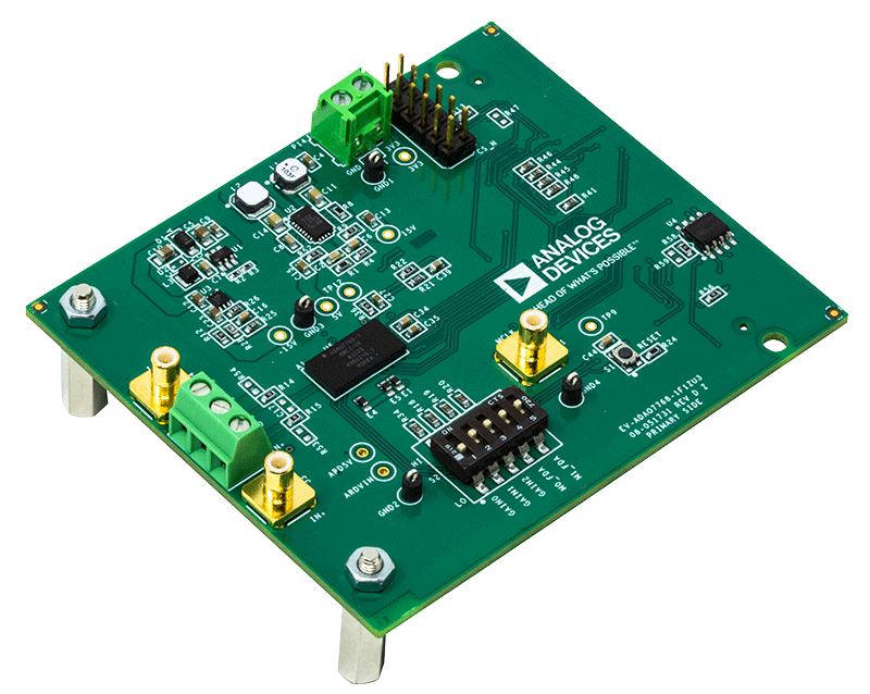


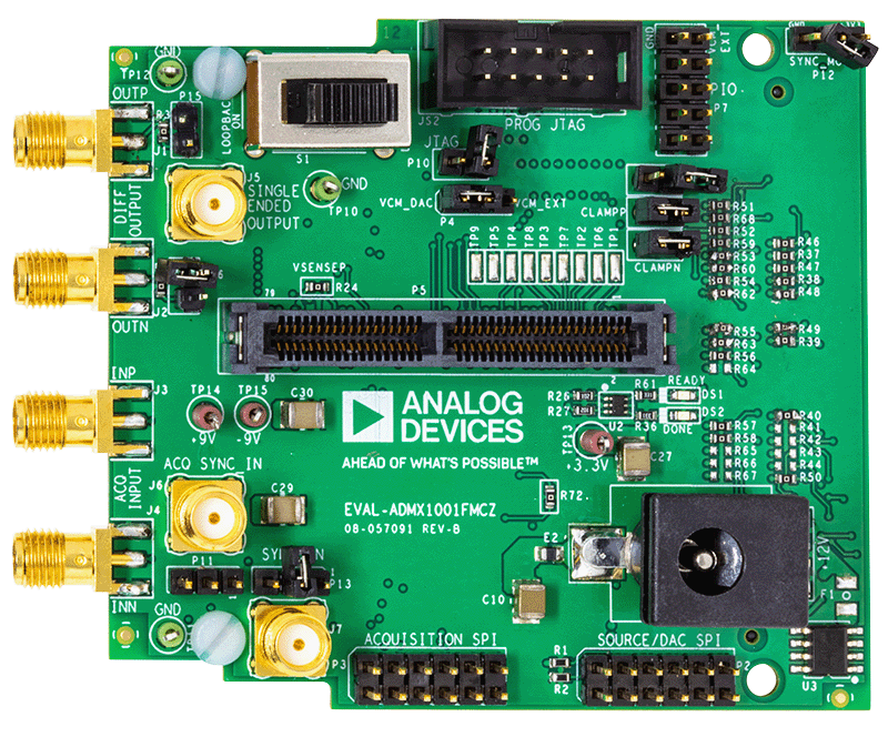
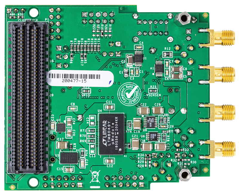
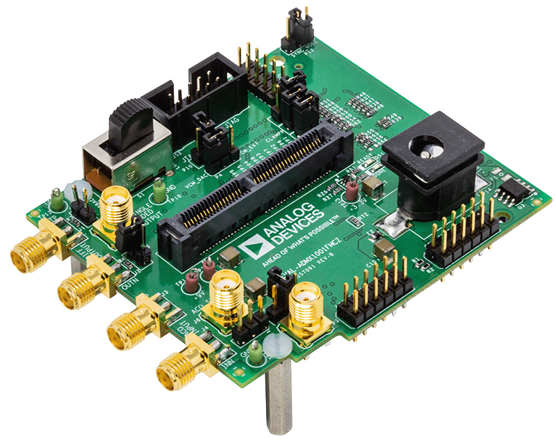
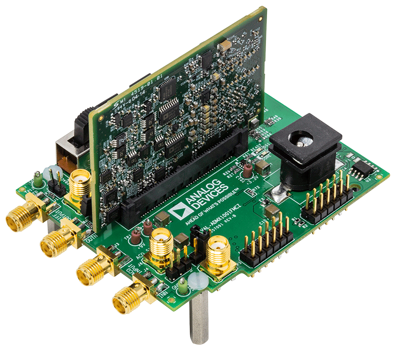
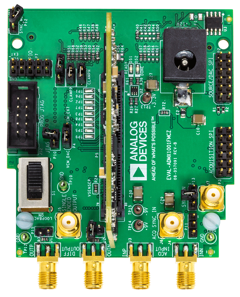
Evaluating the ADAQ7768-1 24-Bit, Single-Channel Precision μModule Data Acquisition System
Resources
Ultra-low Distortion Signal Generator Measurement Module with Fully Differential Input Acquisition Channel
Resources
Software
Latest Discussions
No discussions on ADAQ7768-1 yet. Have something to say?
Start a Discussion on EngineerZone®