ADAQ4001
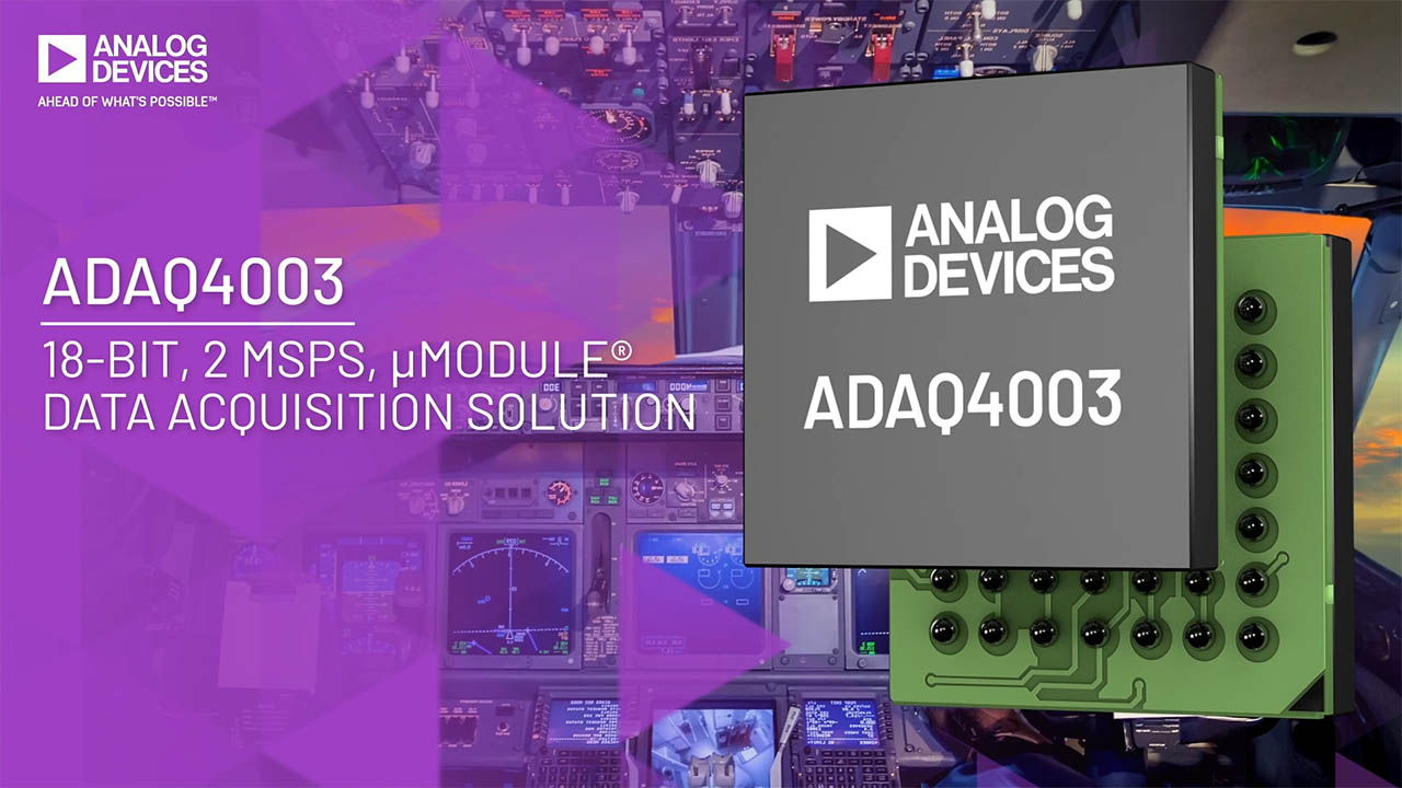
RECOMMENDED FOR NEW DESIGNS16-Bit, 2 MSPS, μModule Data Acquisition Solution
- Part Models
- 2
- 1ku List Price
- Starting From $13.25
Part Details
- Improved design journey
- Fully differential ADC driver with selectable input range
- Input ranges with 5 V VREF: ±10 V, ±5 V, or ±2.5 V
- Essential passive components included
- ±0.005% iPassives matched resistor array
- Wide input common-mode voltage range
- High common-mode rejection ratio
- Single-ended to differential conversion
- Increased signal chain density
- Small, 7 mm × 7 mm, 0.80 mm pitch, 49-ball CSP_BGA
- 4× footprint reduction vs. discrete solution
- On-board reference buffer with VCM generation
- High performance
- Throughput: 2 MSPS, no pipeline delay
- Guaranteed 16-bit no missing codes
- INL: ±4.6 ppm typical, ±11.9 ppm guaranteed
- SINAD: 95 dB typical (G = 0.454)
- Offset error drift: 0.7 ppm/°C typical (G = 0.454)
- Gain error drift: ±0.5 ppm/°C typical
- Low total power dissipation: 51.6 mW typical at 2 MSPS
- SPI-/QSPI™ -/MICROWIRE™ -/DSP-compatible serial interface
- Versatile logic interface supply with 1.8 V, 2.5 V, 3 V, or 5 V
The ADAQ4001 is a μModule® precision data acquisition (DAQ), signal chain solution that reduces the development cycle of a precision measurement system by transferring the signal chain design challenge of component selection, optimization, and layout from the designer to the device.
Using system-in-package (SIP) technology, the ADAQ4001 reduces end system component count by combining multiple common signal processing and conditioning blocks into a single device. These blocks include a high resolution 16-bit, 2 MSPS successive approximation register (SAR), analog-to-digital converter (ADC), a low noise, fully differential ADC driver amplifier (FDA), and a stable reference buffer.
Using Analog Devices, Inc., iPassives® technology, the ADAQ4001 also incorporates crucial passive components with superior matching and drift characteristics to minimize temperature dependent error sources and to offer optimized performance (see Figure 1 in the data sheet). Housing this signal chain solution in a small, 7 mm × 7 mm, 0.80 mm pitch, 49-ball CSP_BGA enables compact form factor designs without sacrificing performance and simplifies end system bill of materials management. This level of system integration makes the ADAQ4001 much less sensitive to printed circuit board (PCB) layout while still providing flexibility to adapt to a wide range of signal levels.
The serial peripheral interface (SPI)-compatible, serial user interface is compatible with 1.8 V, 2.5 V, 3 V, or 5 V logic, using a separate VIO supply. Specified operation of the ADAQ4001 is from −40°C to +125°C.
APPLICATIONS
- Automatic test equipment
- Machine automation
- Process controls
- Medical instrumentation
- Digital control loops
Documentation
Data Sheet 1
User Guide 1
Technical Articles 2
Video 4

Device Drivers 1
3rd Party Solutions 1
Analog Dialogue 1
ADI has always placed the highest emphasis on delivering products that meet the maximum levels of quality and reliability. We achieve this by incorporating quality and reliability checks in every scope of product and process design, and in the manufacturing process as well. "Zero defects" for shipped products is always our goal. View our quality and reliability program and certifications for more information.
| Part Model | Pin/Package Drawing | Documentation | CAD Symbols, Footprints, and 3D Models |
|---|---|---|---|
| ADAQ4001BBCZ | 49-Ball CSPBGA (7mm x 7mm) | ||
| ADAQ4001BBCZ-RL13 | 49-Ball CSPBGA (7mm x 7mm) |
This is the most up-to-date revision of the Data Sheet.
Software Resources
ADAQ4003: FPGA Device Driver
Device Drivers 1
Evaluation Software 0
Can't find the software or driver you need?
Hardware Ecosystem
| Parts | Product Life Cycle | Description |
|---|---|---|
| Boost Regulators & Controllers 1 | ||
| ADP5070 | RECOMMENDED FOR NEW DESIGNS | 1 A/0.6 A, DC-to-DC Switching Regulator with Independent Positive and Negative Outputs |
| High Speed Op Amps 4 | ||
| ADA4807-1 | RECOMMENDED FOR NEW DESIGNS |
3.1 nV/√Hz, 1 mA, 180 MHz, Rail-to-Rail Input/Output Amplifier |
| AD8031 | PRODUCTION | 2.7 V, 800 µA, 80 MHz Rail-to-Rail I/O Single Amplifier |
| ADA4898-1 | PRODUCTION | High Voltage, Low Noise, Low Distortion, Unity Gain Stable, High Speed Op Amp |
| ADA4898-2 | PRODUCTION | High Voltage, Low Noise, Low Distortion, Unity Gain Stable, High Speed, Dual 8-Lead Op Amp |
| Instrumentation Amplifiers 2 | ||
| AD8251 | PRODUCTION | 10 MHz, G = 1, 2, 4, 8 iCMOS® Programmable Gain Instrumentation Amplifier |
| LTC6373 | RECOMMENDED FOR NEW DESIGNS | 36V Fully-Differential Programmable-Gain Instrumentation Amplifier with 25pA Input Bias Current |
| Interface Transceivers & Isolators 2 | ||
| ADUM141D | RECOMMENDED FOR NEW DESIGNS |
Robust, Quad Channel Isolator W/ Input Disable & 1 Reverse Channel |
| ADUM141E | RECOMMENDED FOR NEW DESIGNS |
Robust, Quad Channel Isolator W/ Output Enable & 1 Reverse Channel |
| Linear Regulators 2 | ||
| LT3023 | RECOMMENDED FOR NEW DESIGNS | Dual 100mA, Low Dropout, Low Noise, Micropower Regulator |
| ADP7118 | RECOMMENDED FOR NEW DESIGNS | 20 V, 200 mA, Low Noise, CMOS LDO Linear Regulator |
| Voltage References 12 | ||
| ADR3450 | PRODUCTION | Micro-Power, High-Accuracy 5.0V Voltage Reference |
| ADR3440 | PRODUCTION | Micro-Power, High-Accuracy 4.096V Voltage Reference |
| ADR3533 | RECOMMENDED FOR NEW DESIGNS | Micropower, Precision, Auto Qualified 3.3V Voltage Reference |
| ADR3525 | RECOMMENDED FOR NEW DESIGNS | Micropower, Precision, Auto Qualified 2.5V Voltage Reference |
| ADR4550 | RECOMMENDED FOR NEW DESIGNS | Ultra-Low-Noise, High-Accuracy 5.0V Voltage Reference |
| ADR4540 | RECOMMENDED FOR NEW DESIGNS | Ultra-Low-Noise, High-Accuracy 4.096V Voltage Reference |
| ADR4533 | RECOMMENDED FOR NEW DESIGNS | Ultra-Low-Noise, High-Accuracy 3.3V Voltage Reference |
| ADR4525 | RECOMMENDED FOR NEW DESIGNS | Ultra-Low-Noise, High-Accuracy 2.5V Voltage Reference |
| ADR444 | PRODUCTION | Ultralow Noise, LDO XFET® 4.096V Voltage Reference w/Current Sink and Source |
| ADR445 | PRODUCTION | Ultralow Noise, LDO XFET® 5.0V Voltage Reference w/Current Sink and Source |
| ADR441 | PRODUCTION | Ultralow Noise, LDO XFET® 2.5V Voltage Reference w/Current Sink and Source |
| LTC6655 | PRODUCTION | 0.25ppm Noise, Low Drift Precision References |
Tools & Simulations
IBIS Model 1
Signal Chain Designer - BETA
Signal Chain Designer is a web-based tool designed to create and simulate complex precision signal chains. See your circuit’s performance before you commit to your PCB: transfer function, noise, power consumption, input range, and DC error. Quickly experiment with different parts and architectures. Signal chains can be exported to LTspice for further analysis.
Open ToolEvaluation Kits
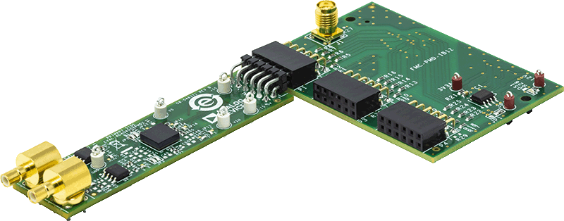
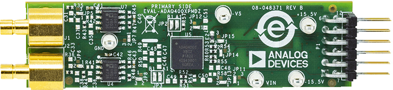
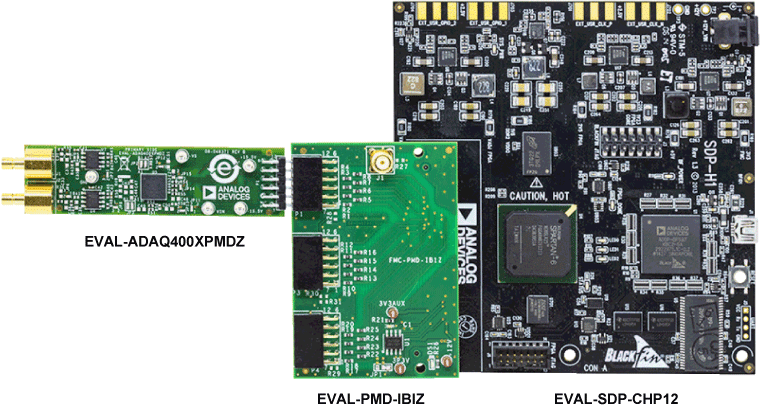
Evaluating the ADAQ4001/ADAQ4003 16-/18-Bit, 2 MSPS, μModule Data Acquisition Solution
Resources
Latest Discussions
No discussions on ADAQ4001 yet. Have something to say?
Start a Discussion on EngineerZone®