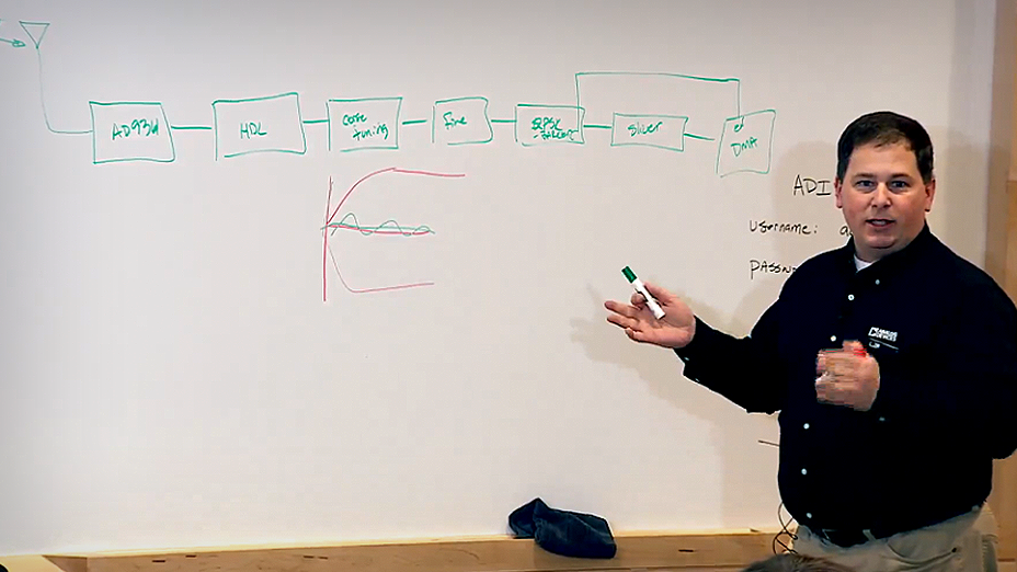
The ADALM-PLUTO is a complete open reference design for SDR that helps you quickly verify your ADI RF product-based designs and get them to production faster. It includes schematics, HDL, firmware, embedded Linux, drivers, and host drivers for ADI’s transceiver products.
Fast track your designAD9361
RECOMMENDED FOR NEW DESIGNSRF Agile Transceiver
- Part Models
- 2
- 1ku List Price
- Starting From $224.70
Part Details
- RF 2 × 2 transceiver with integrated 12-bit DACs and ADCs
- TX band: 47 MHz to 6.0 GHz
- RX band: 70 MHz to 6.0 GHz
- Supports TDD and FDD operation
- Tunable channel bandwidth: <200 kHz to 56 MHz
- Dual receivers: 6 differential
- Superior receiver sensitivity with a noise figure of 2 dB at 800 MHz LO
- RX gain control
- Real-time monitor and control signals for manual gain
- Independent automatic gain control
- Dual transmitters: 4 differential outputs
- Highly linear broadband transmitter
- TX EVM: ≤−40 dB
- TX noise: ≤−157 dBm/Hz noise floor
- TX monitor: ≥66 dB dynamic range with 1 dB accuracy
- Integrated fractional-N synthesizers
- 2.4 Hz maximum local oscillator (LO) step size
- Multichip synchronization
- CMOS/LVDS digital interface
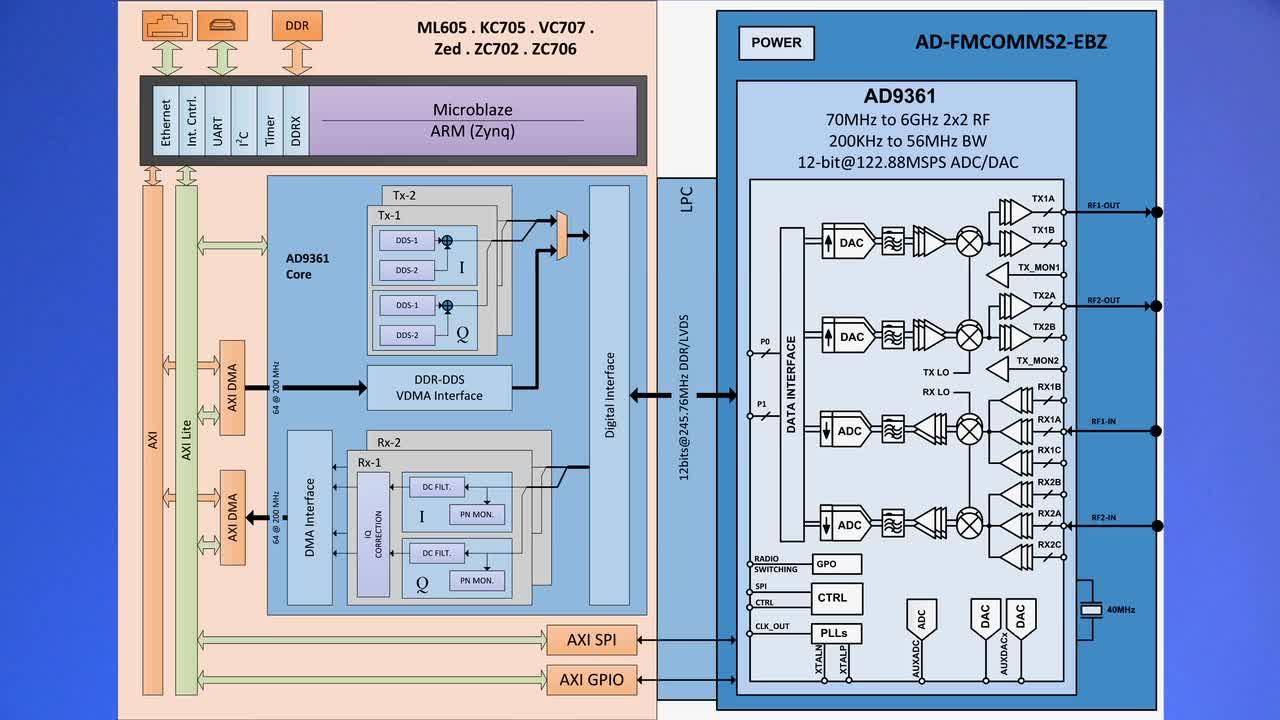
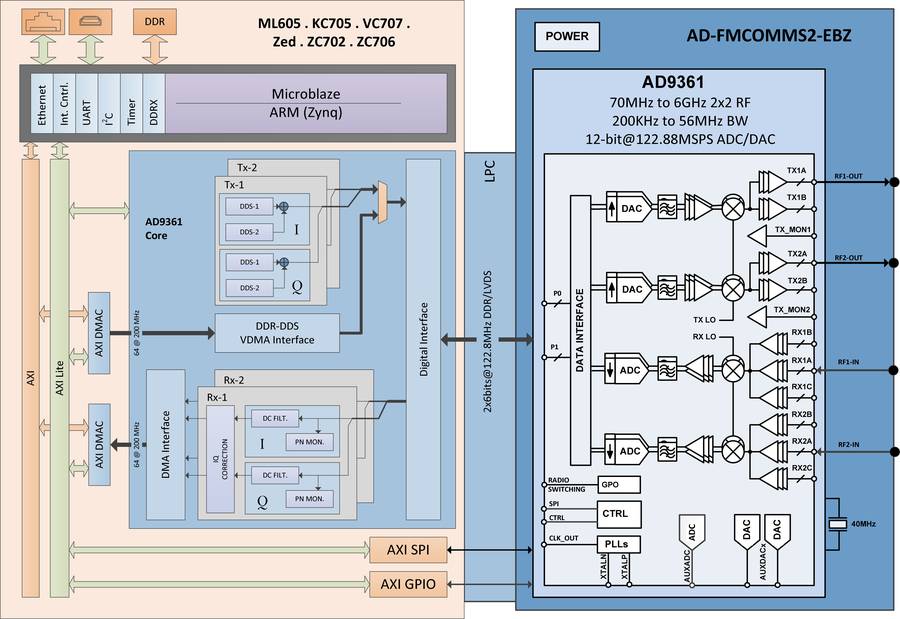
The AD9361 is a high performance, highly integrated radio frequency (RF) Agile Transceiver™ designed for use in 3G and 4G base station applications. Its programmability and wideband capability make it ideal for a broad range of transceiver applications. The device combines a RF front end with a flexible mixed-signal baseband section and integrated frequency synthesizers, simplifying design-in by providing a configurable digital interface to a processor. The AD9361 receiver LO operates from 70 MHz to 6.0 GHz and the transmitter LO operates from 47 MHz to 6.0 GHz range, covering most licensed and unlicensed bands. Channel bandwidths from less than 200 kHz to 56 MHz are supported.
The two independent direct conversion receivers have state-of-the-art noise figure and linearity. Each receive (RX) subsystem includes independent automatic gain control (AGC), dc offset correction, quadrature correction, and digital filtering, thereby eliminating the need for these functions in the digital baseband. The AD9361 also has flexible manual gain modes that can be externally controlled. Two high dynamic range analog-to-digital converters (ADCs) per channel digitize the received I and Q signals and pass them through configurable decimation filters and 128-tap finite impulse response (FIR) filters to produce a 12-bit output signal at the appropriate sample rate.
The transmitters use a direct conversion architecture that achieves high modulation accuracy with ultralow noise. This transmitter design produces a best in class TX error vector magnitude (EVM) of <−40 dB, allowing significant system margin for the external power amplifier (PA) selection. The on-board transmit (TX) power monitor can be used as a power detector, enabling highly accurate TX power measurements.
The fully integrated phase-locked loops (PLLs) provide low power fractional-N frequency synthesis for all receive and transmit channels. Channel isolation, demanded by frequency division duplex (FDD) systems, is integrated into the design. All VCO and loop filter components are integrated.
The core of the AD9361 can be powered directly from a 1.3 V regulator. The IC is controlled via a standard 4-wire serial port and four real-time input/output control pins. Comprehensive power-down modes are included to minimize power consumption during normal use. The AD9361 is packaged in a 10 mm × 10 mm, 144-ball chip scale package ball grid array (CSP_BGA).
Applications
- Point to point communication systems
- Femtocell/picocell/microcell base stations
- General-purpose radio systems
Documentation
Data Sheet 1
User Guide 2
Application Note 2
Technical Articles 10
Informational 1
Video 22


Solutions Bulletin & Brochure 2
Device Drivers 2
3rd Party Solutions 1
Analog Dialogue 11
Webcast 6
ADI has always placed the highest emphasis on delivering products that meet the maximum levels of quality and reliability. We achieve this by incorporating quality and reliability checks in every scope of product and process design, and in the manufacturing process as well. "Zero defects" for shipped products is always our goal. View our quality and reliability program and certifications for more information.
| Part Model | Pin/Package Drawing | Documentation | CAD Symbols, Footprints, and 3D Models |
|---|---|---|---|
| AD9361BBCZ | 144-Ball CSPBGA (10mm x 10mm x 1.7mm) | ||
| AD9361BBCZ-REEL | 144-Ball CSPBGA (10mm x 10mm x 1.7mm) |
This is the most up-to-date revision of the Data Sheet.
Software Resources
Evaluation Software 0
Hardware Ecosystem
| Parts | Product Life Cycle | Description |
|---|---|---|
| Digital-to-Analog Converters (DACs) 1 | ||
| AD9548 | RECOMMENDED FOR NEW DESIGNS | Quad/Octal Input Network Clock Generator/Synchronizer |
| LDO Linear Regulators 1 | ||
| ADP1755 | PRODUCTION | 1.2A Low-Vin, Adjustable-Vout LDO Linear Regulator |
| Low-Noise Amplifiers (LNAs) & Power Amplifiers 6 | ||
| ADL5602 | RECOMMENDED FOR NEW DESIGNS | 50 MHz TO 4.0 GHz RF/IF Gain Block |
| ADL5521 | RECOMMENDED FOR NEW DESIGNS | 400 MHz TO 4000 MHz Low Noise Amplifier |
| ADL5523 | RECOMMENDED FOR NEW DESIGNS | 400 MHz TO 4000 MHz Low Noise Amplifier |
| ADL5320 | RECOMMENDED FOR NEW DESIGNS | 400 MHz TO 2700 MHz ¼ Watt RF Driver Amplifier |
| ADL5321 | RECOMMENDED FOR NEW DESIGNS | 2.3 GHz TO 4.0 GHz ¼ Watt RF Driver Amplifier |
| ADL5324 | RECOMMENDED FOR NEW DESIGNS | 400 MHz TO 4000 MHz ½ Watt RF Driver Amplifier |
| Phase-Locked Loop (PLL) Synthesizers 1 | ||
| ADF4351 | RECOMMENDED FOR NEW DESIGNS | Wideband Synthesizer with Integrated VCO |
| Switching Regulators & Controllers 2 | ||
| ADP5040 | RECOMMENDED FOR NEW DESIGNS | Micro PMU with 1.2 A Buck Regulator and Two 300 mA LDOs |
| ADP2164 | RECOMMENDED FOR NEW DESIGNS | 6.5V, 4 A, High Efficiency, Step-Down DC-to-DC Regulator |
Tools & Simulations
SDR Integrated Transceiver Design Resources
This site contains the device documentation packages for the SDR Integrated Transceivers including user guides, IBIS models, and PCB files.
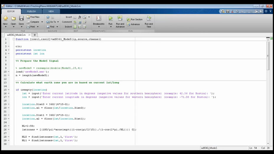
Open ToolMATLAB Filter Design Wizard for AD9361
Open Tool
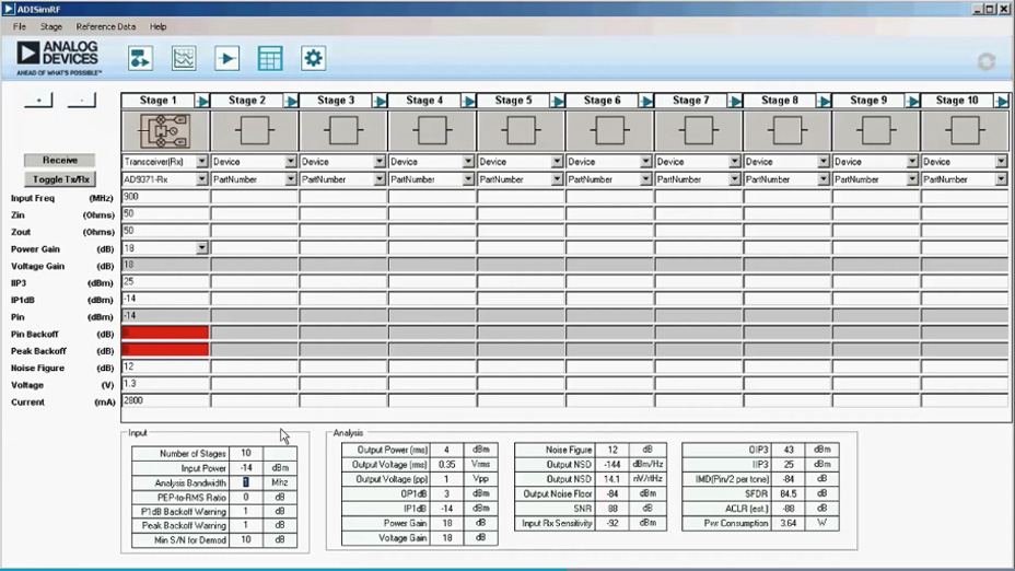
ADIsimRF
ADIsimRF is an easy-to-use RF signal chain calculator. Cascaded gain, noise, distortion and power consumption can be calculated, plotted and exported for signal chains with up to 50 stages. ADIsimRF also includes an extensive data base of device models for ADI’s RF and mixed signal components.
Open ToolEvaluation Kits

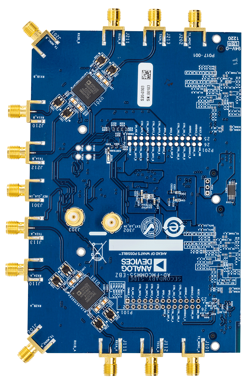
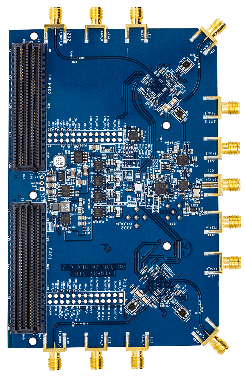
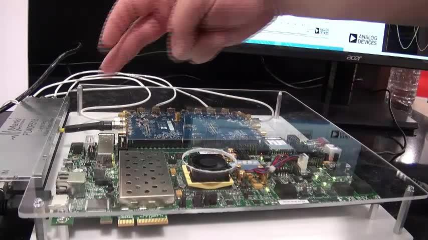
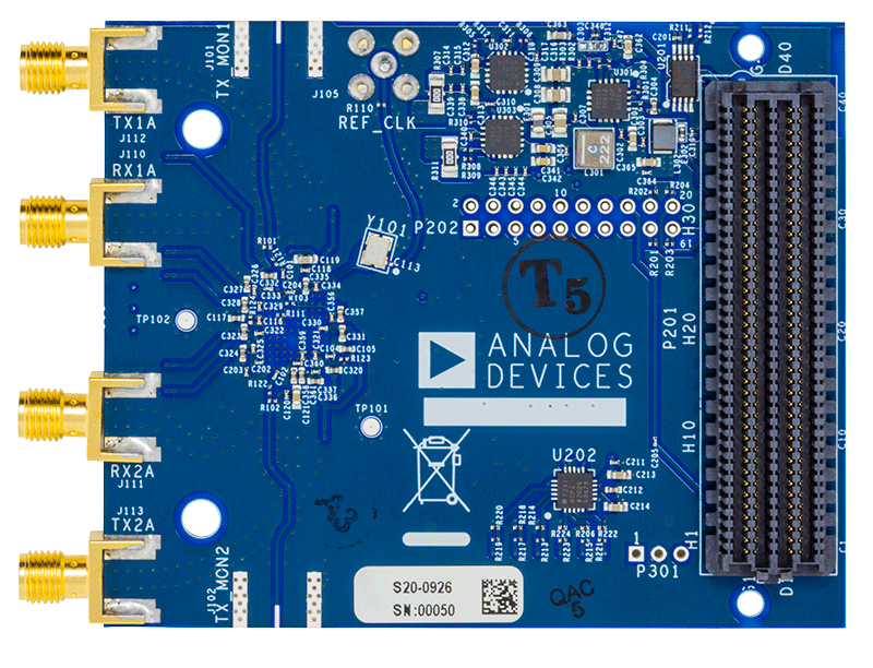
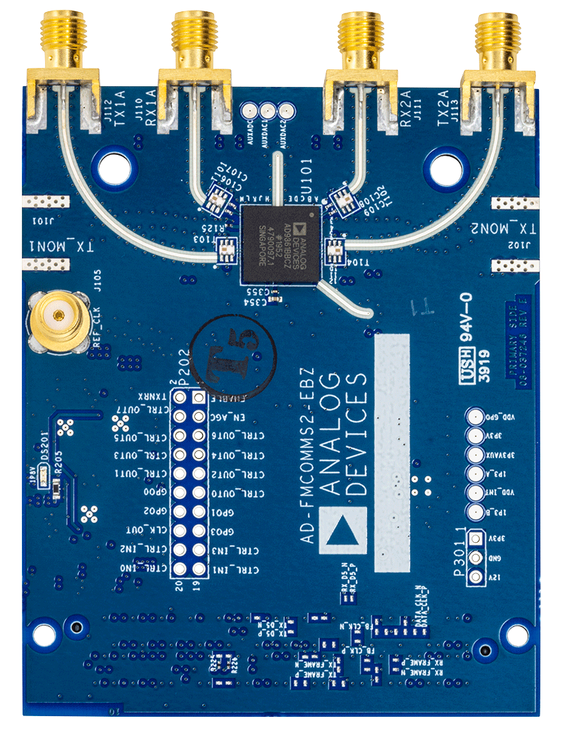
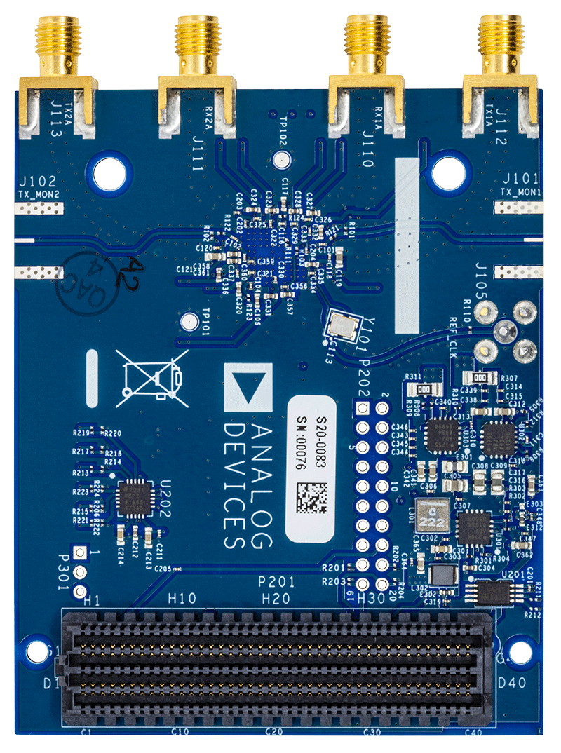
Dual AD9361 Evaluation Board
Resources

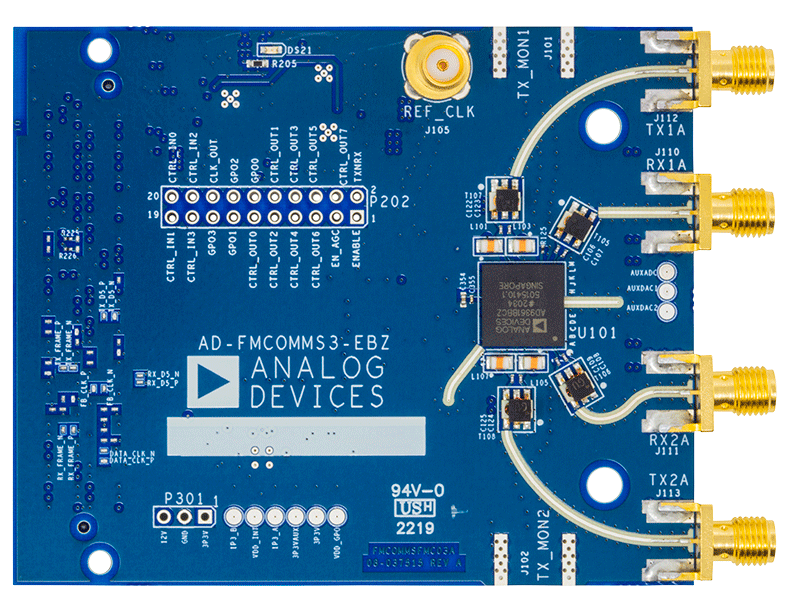
AD9361 Wideband Software Defined Radio Board
Resources
Software

AD9361 Software Defined Radio Board (2.4GHz Optimized)
Resources
Software

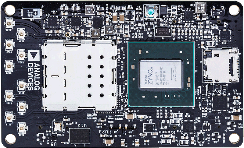
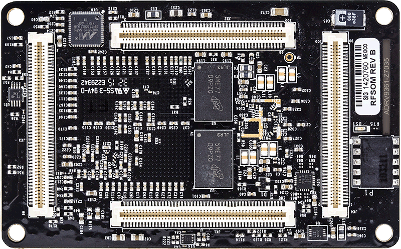
SDR 2x2 System-On-Module
Resources
Reference Designs
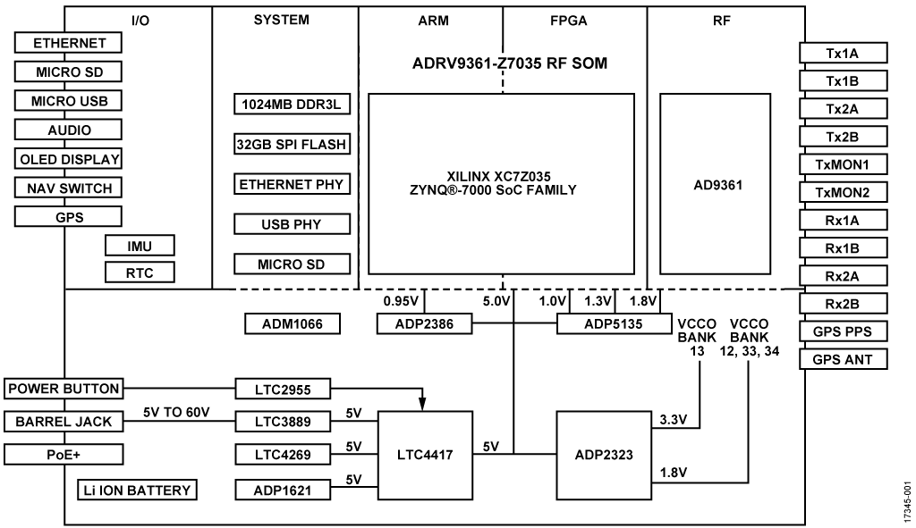
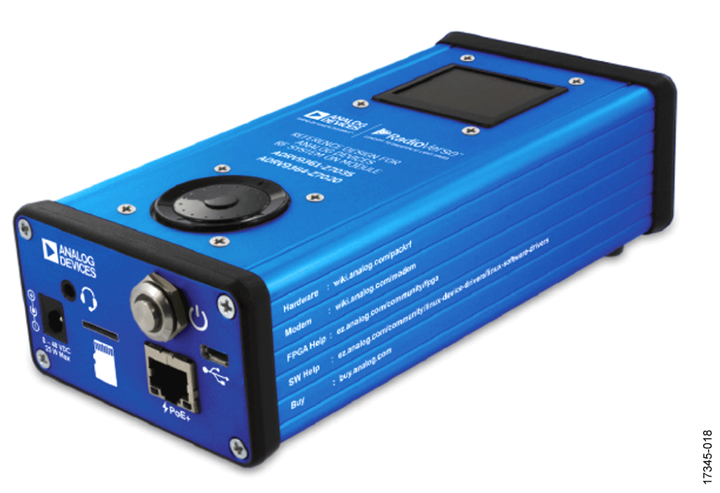
ADRV-PACKRF Robust Portable Radio Design
Part Used
Design & Integration Tools
Latest Discussions
No discussions on AD9361 yet. Have something to say?
Start a Discussion on EngineerZone®