ADA4352-2
预发布Dual-Channel, Precision, Programmable Gain Transimpedance Amplifier (PGTIA) with Integrated Gain Resistors
- 产品模型
- 3
产品详情
- Small, dual-channel, complete PGTIA and AFE solution
- Small size package: 16-lead LFCSP, 3 mm × 3 mm
- Integrated four internal gains per channel
- Range 0, internal RF = 315 Ω
- Range 1, internal RF = 3.5 kΩ
- Range 2, internal RF = 40.2 kΩ
- Range 3, internal RF = 450 kΩ
- Wide input current dynamic ranges from 100 picoamps to milliamps
- Excellent DC precision
- Low offset voltage: ±100 μV maximum, 25°C
- Low offset voltage drift: ±0.85 μV/°C maximum, −40°C to +125°C
- Low switch integrated switch impedance 19Ω maximum, −40°C to +125°C
- Excellent dynamic performance
- Range 0 settling time 1 µs
- Range 1 settling time 2 µs
- Range 2 settling time 5 µs
- Range 3 settling time 10 µs
- Kelvin-connected architecture eliminates gain error due to switch resistance over temperature.
- Single-supply operation: +2.7 V to +5.5 V (dual-supply operation: ±1.85 V to ±2.75 V)
- Wide gain bandwidth product: 8.5 MHz
- Wide operating temperature range: −40°C to +125°C
The ADA4352-2 is a compact, monolithic, dual-channel, precision, programmable gain transimpedance amplifier (PGTIA). The ADA4352-2 is a breakthrough solution for precisely measuring small currents over a wide dynamic range. The precision of the ADA4352-2 over a wide temperature range of −40°C to +125°C enables users to perform one calibration of the end equipment at room temperature, thereby saving test time and cost. The ADA4352-2 integrates four current-to-voltage gain selections per channel, and the gain is programmable using two logic pins per channel to provide a flexible, fully functional compact PGTIA solution. Additionally, with its robust output stage and low noise, the ADA4352-2 can directly drive 16-bit precision analog-to-digital converters (ADCs, such as AD4696), providing a complete analog front-end (AFE) to address the most challenging precision current measurement applications.
The ADA4352-2 is offered in a 3 mm × 3 mm LFCSP, reducing the printed circuit board (PCB) area by up to 10 times relative to a discrete design using standalone operational amplifiers (op amps) and switches.
Applications
- Precision current to voltage (I to V) conversion
- Programmable gain TIAs
- Photodetector interface and amplification
- Optical networking equipment
- Optical power measurement
- Instrumentation—spectroscopy and chromatography
- Precision data acquisition systems (DAQ)
参考资料
数据手册 1
用户手册 1
视频 2


ADI 始终高度重视提供符合最高质量和可靠性水平的产品。我们通过将质量和可靠性检查纳入产品和工艺设计的各个范围以及制造过程来实现这一目标。出货产品的“零缺陷”始终是我们的目标。查看我们的质量和可靠性计划和认证以了解更多信息。
| 产品型号 | 引脚/封装图-中文版 | 文档 | CAD 符号,脚注和 3D模型 |
|---|---|---|---|
| ADA4352-2ACPZ | LFCSP:LEADFRM CHIP SCALE | ||
| ADA4352-2ACPZ-R7 | LFCSP:LEADFRM CHIP SCALE | ||
| ADA4352-2ACPZ-RL | LFCSP:LEADFRM CHIP SCALE |
这是最新版本的数据手册
软件资源
找不到您所需的软件或驱动?
申请驱动/软件硬件生态系统
| 部分模型 | 产品周期 | 描述 |
|---|---|---|
| ADA4351-2 | 推荐新设计使用 | 紧凑型、双通道、精密、可编程增益跨阻放大器(PGTIA) |
评估套件
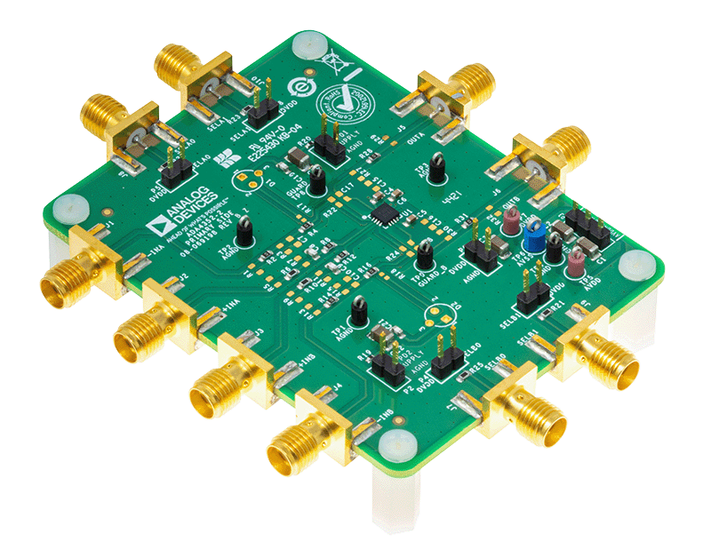
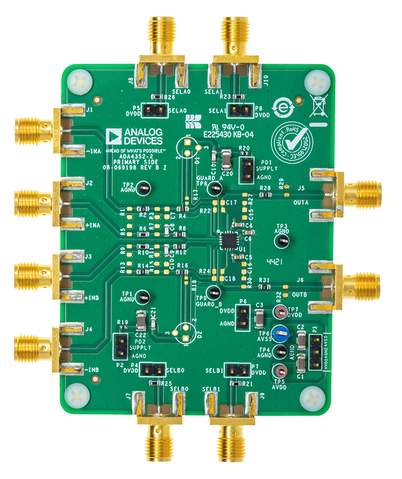
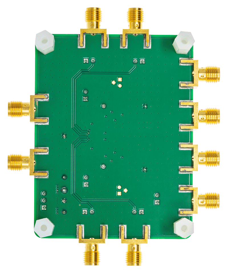
ADA4352-2 评估板用户指南
资料
最新评论
需要发起讨论吗? 没有关于 ADA4352-2的相关讨论?是否需要发起讨论?
在EngineerZone®上发起讨论