ADN4622
RECOMMENDED FOR NEW DESIGNS5.7 kV rms/1.5 kV rms, Quad-Channel LVDS 2.5 Gigabit Isolators (2 Reverse Channels)
- Part Models
- 4
- 1ku List Price
- Starting From $15.89
Part Details
- 5.7 kV rms and 1.5 kV rms LVDS isolators
- Complies with TIA/EIA-644-A LVDS signal levels
- Quad-channel configuration (ADN4622: 2 + 2, ADN4624: 4 + 0)
- Any data rate up to 2.5 Gbps switching with low jitter
- 10 Gbps total bandwidth across four channels
- 2.15 ns typical propagation delay
- Typical jitter: 0.82 ps rms random, 40 ps total peak
- Lower power 1.8 V supplies
- ±8 kV IEC 61000-4-2 ESD protection across isolation barrier
- High common-mode transient immunity: 100 kV/μs typical
- Safety and regulatory approvals (28-lead SOIC_W_FP package)
- UL (pending): 5700 V rms for 1 minute per UL 1577
- CSA Component Acceptance Notice 5A (pending)
- VDE certificate of conformity (pending)
- DIN V VDE V 0884-11 (VDE V 0884-11):2017-01
- VIORM = 849 VPEAK (working voltage)
- Enable or disable refresh (low-speed output correctness check)
- Operating temperature range: −40°C to +125°C
- 28-lead, wide-body, finer pitch SOIC_W_FP package with 8.3 mm creepage and clearance or 6 mm × 6 mm LFCSP package with 1.27 mm creepage and clearance
The ADN4622/ADN4624 are quad-channel, signal isolated, low-voltage differential signaling (LVDS) buffers that operate at up to 2.5 Gbps with very low jitter. The devices integrate Analog Devices, Inc., iCoupler® technology, enhanced for high-speed operation to provide drop-in galvanic isolation of LVDS signal chains. AC coupling and/or level shifting to the LVDS receivers and from the LVDS drivers allows isolation of other high-speed signals such as current-mode logic (CML).
The ADN4622/ADN4624 include a refresh mechanism to monitor the input and output states and ensure they remain the same in the absence of data transitions. For lower power consumption and high-speed operation with low jitter, the LVDS and isolator circuits rely on 1.8 V supplies. The ADN4622/ADN4624 are fully specified over a wide industrial temperature range and are available in a 28-lead, wide-body, finer pitch SOIC_W_FP package with 8.3 mm creepage and clearance (for 5.7 kV rms or 8 kVPEAK surge and impulse voltages and reinforced insulation at AC mains voltages) or 6 mm × 6 mm LFCSP package with 1.27 mm creepage and clearance (for basic/functional isolation).
APPLICATIONS
- Isolated video and imaging data
- Analog front-end isolation
- Data plane isolation
- Isolated high speed clock and data links
- Multi-gigabit SERDES
- Board-to-board optical replacement (for example, short reach fiber)
Documentation
Data Sheet 1
User Guide 1
Safety and Regulatory Compliance 1
Safety and Regulatory Compliance 1
ADI has always placed the highest emphasis on delivering products that meet the maximum levels of quality and reliability. We achieve this by incorporating quality and reliability checks in every scope of product and process design, and in the manufacturing process as well. "Zero defects" for shipped products is always our goal. View our quality and reliability program and certifications for more information.
| Part Model | Pin/Package Drawing | Documentation | CAD Symbols, Footprints, and 3D Models |
|---|---|---|---|
| ADN4622BCPZ | 32-Lead LFCSP (6 mm x 6 mm x 0.75 mm) | ||
| ADN4622BCPZ-RL | 32-Lead LFCSP (6 mm x 6 mm x 0.75 mm) | ||
| ADN4622BRNZ | 28-Lead SOIC (Wide, Finer Pitch) | ||
| ADN4622BRNZ-RL | 28-Lead SOIC (Wide, Finer Pitch) |
This is the most up-to-date revision of the Data Sheet.
Evaluation Kits
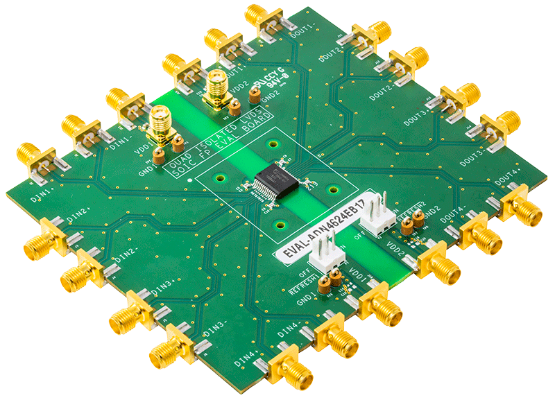
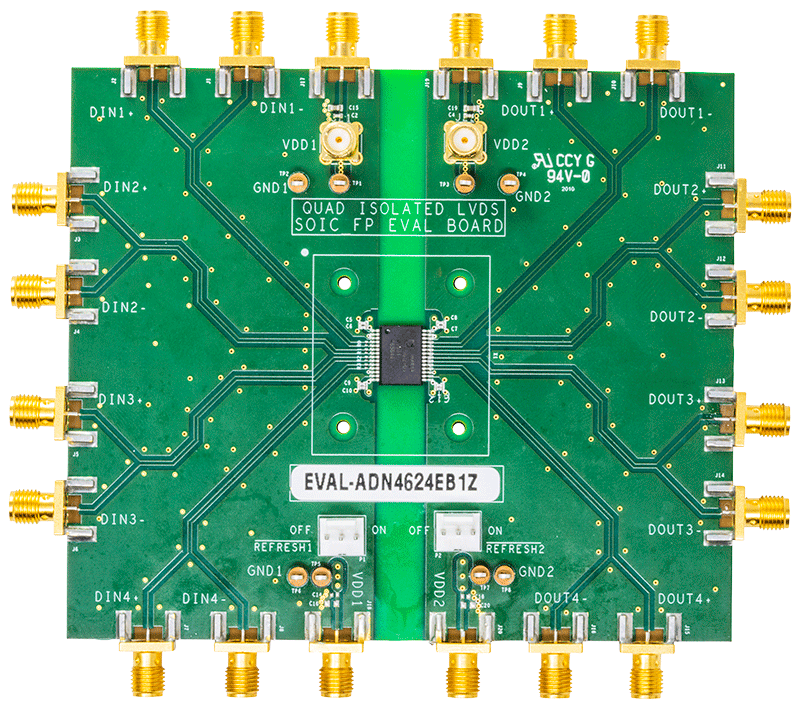
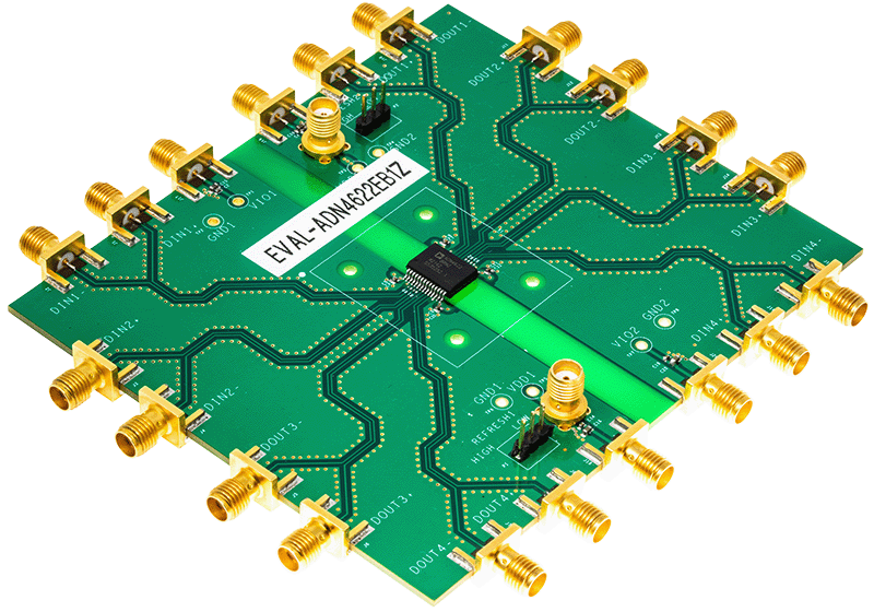

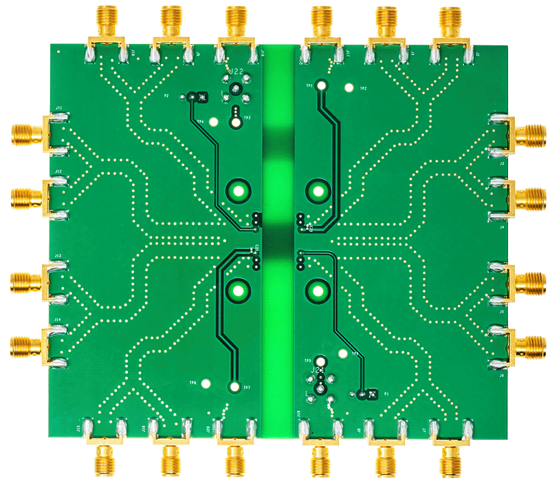
Evaluating the ADN4622/ADN4624 5.7 kV rms/1.5 kV rms, Quad-Channel LVDS 2.5 Gigabit Isolators
Resources
Latest Discussions
No discussions on ADN4622 yet. Have something to say?
Start a Discussion on EngineerZone®