A quality frequency source (i.e., oscillator) is often required for applications such as the local oscillator (LO) in a wireless handset, the frequency reference in a phase-locked LO, or the master clock source in a microprocessor or data-acquisition system.
For a system designer, the important signal-source parameters are frequency accuracy and frequency stability. Accuracy pertains to the initial value of frequency, and stability pertains to the frequency's phase noise (short-term) and drift (long-term) as affected by temperature and aging. For a crystal-oscillator designer, the key parameters are those of the resonator itself: resonant frequency, reactance, and Q-factor. With the possible exception of phase noise, these parameters are almost entirely a function of the crystal.
Low phase noise depends on the resonator and the active element. The resonator should have high Q (most crystals have an extremely high Q in the 10,000 to 50,000 range). The active element should have low flicker noise and low noise figure, and its loading on the resonator should be minimal. Such attributes describe the active device in a MAX2620 IC: it exhibits the low flicker noise inherent in a high-frequency bipolar process, a low noise figure, and a low parasitic rb, whose minimal load on the active device maintains the high loaded Q desired in an oscillator circuit. Figure 1 shows a simple crystal oscillator.
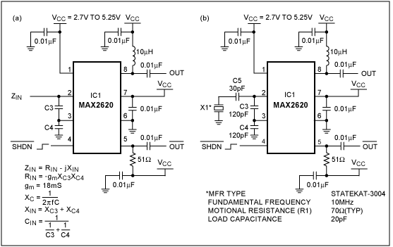
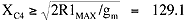
Figure 1. This simple crystal oscillator is based on a single oscillator IC. The crystal resonator, X1, is shown in (b).
Other MAX2620 features desirable in an active-oscillator element include buffer amplifiers that minimize load-pulling on the oscillator frequency, operation over supply voltages in the +2.7V to +5.25V range, supply-insensitive internal biasing, shutdown capability, and two open-collector outputs that can be configured as two single-ended outputs or a single differential output.
The primary criteria for selecting a crystal resonator are nominal frequency, initial frequency accuracy, and frequency stability vs. temperature and aging. In practice, a designer should take note of the crystal resonator's center frequency, Q, motional resistance, and load capacitance. These parameters enable the designer to calculate values for the oscillator circuit's external capacitors.
In Figure 1b, the crystal resonator (X1) is a surface-mount, fundamental-mode device from Statek. The motional-resistance value is needed to calculate values for C3 and C4 in Figure 1a, but the worst-case (high) value is preferred to the typical value. In this case, the device manufacturer specifies a maximum motional resistance of 150Ω. For oscillation to start, this value should be less than the magnitude of input negative resistance (RIN = -gmXC3XC4) for the active device; refer to Figure 1a. As a matter of good practice, it should be less than half. Therefore,
gmXC3XC4 > 2R1MAX
where
gm is the active-device transconductance. In this case, it equals 18mS (18 milli-Siemens).
XC3 is the reactance of capacitor C3 (1/2πfC3).
XC4 is the reactance of capacitor C4 (1/2πfC4).
R1MAX (150Ω) is the crystal resonator's maximum motional resistance.
Rearranging and choosing XC3 = XC4,
At 10MHz, the value for C3 and C4 (assumed equal) is:
C3 = C4 = 1/2πfXC4 = 123.3pF
Choosing an industry-standard capacitor value of 120pF, the load capacitance across the crystal resonator is the series connection of C3 and C4: 1/(1/C3 + 1/C4) = 60pF. To ensure oscillation at the desired frequency, however, the crystal resonator must be loaded by its specified load capacitance (20pF). This can be achieved by decreasing the value of C3 and C4 to 40pF each, but the result is a very large excess gain (RIN + R1MAX) that may be detrimental to the oscillator's noise performance. The preferred method for setting a 20pF net load capacitance is to introduce a 30pF series capacitor (C5 in the completed circuit of Figure 1b).
The open-collector pins active-low OUT and OUT (pins 5 and 8) provide either a differential output or two single-ended outputs. Each pin can sink about 2.5mA of quiescent current, and each requires a pull-up to VCC. Either an RF choke or a resistor can serve as the pull-up, but for differential outputs be sure to use the same type on each line. Note that resistive pull-ups greater than 100Ω cause an excessive voltage drop. For 50Ω loads, the single-ended output level is about -6dBm (320mVP-P) with an RF-choke pull-up, and about -13dBm (140mVP-P) with a 50Ω resistive pull-up.
A similar idea appeared in the April 1998 issue of Microwaves and RF.
Related to this Article
Products
Product Categories
Latest Media 21