Abstract
The MAX3420E makes it easy to design a USB peripheral using a general-purpose microcontroller. After introducing the MAX3420E, this article focuses on the device's SPI interface. The article demonstrates how to access the device either by using a hardwired SPI unit or by bit-banging general-purpose I/O pins. Example C code is given for a USB design that uses the MAXQ2000 microcontroller.
Introduction
Articles about the Universal Serial Bus (USB) used to start by justifying USB as the new connection standard for personal computers. Thankfully that is no longer necessary, so this introduction can be mercifully short. If you have an embedded system and want to connect to a PC, the mainstream conduit is USB.
A new chip from Analog Devices, the MAX3420E, makes it easy to add USB to any system. This article focuses on the MAX3420E's integrated SPI (Serial Peripheral Interface) interface and provides example C code for a generic SPI implementation. The article concludes with code for a simple USB HID (Human Interface Device), a Windows-based panic button.
Adding USB to Anything
Microcontroller (µC) choices are often made based on integrated peripherals. Some processors include USB functionality, but most, especially the really low-cost versions, do not. Have you ever selected a microcontroller with the perfect combination of I/O and peripherals, but found that it lacks USB? Also, do you want to add USB and continue to use your existing development tools?
It is now possible to add USB to any microcontroller with Analog's new MAX3420E. This chip provides a USB full-speed transceiver, an intelligent USB serial interface engine (SIE), and an SPI slave interface that can run with an SCLK clock signal up to 26MHz. The MAX3420E operates as a full-speed USB peripheral with one control endpoint, two double-buffered 64byte data endpoints, and one 64byte interrupt endpoint.
A Bus-Powered Widget
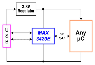
Figure 1. A USB bus-powered widget.
Figure 1 illustrates a common USB peripheral architecture. The USB VBUS wire provides 5V power to a 3.3V regulator, which powers the microcontroller and the MAX3420E to eliminate an external power supply. The SPI interface can comprise 3, 4, or 5 wires. Table 1 shows the full 5-pin interface.
| Signal | MAX3420E Direction | Description |
| MOSI | In | SPI master out, slave in |
| MISO | Out | SPI master in, slave out |
| SCLK | In | Serial clock |
| SS# | In | Slave select |
| INT | Out | Interrupt (level or pulse) |
If the application does not require interrupts (all MAX3420E interrupt conditions can be directly tested by reading register bits), you can leave off the INT pin and have a 4-pin interface. If your SPI master has a bidirectional data interface (MOSI/MISO on the same bidirectional pin) you can reduce the interface by yet another pin. Therefore, an SPI interface with no interrupt support and a bidirectional data pin uses only three pins.
What do you do if the microcontroller does not have an SPI port? No problem. It is very easy to make a firmware-driven SPI master by directly toggling general-purpose I/O pins. A strong feature of USB is that it is self-throttling; it automatically accommodates any speed interface on the SPI side. (It does this by using a NAK handshake on the USB side to indicate, "busy now, try again.") Many USB peripherals, especially those connected to humans, can operate very responsively with even the slowest SPI interface.
What if the microcontroller in Figure 1 is really small, perhaps under 10 pins? Do you need to use all those valuable I/O pins just to talk to the USB chip? Yes, but this is exactly why the MAX3420E provides four general-purpose inputs and four general-purpose outputs. Simply put, the MAX3420E has eight general-purpose I/Os to replace the pins needed to talk to it, but then the MAX3420E adds more I/Os. So your system actually has more I/O pins after connecting a MAX3420E.
A Big Chip
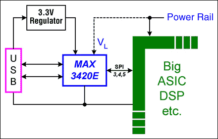
Figure 2. Connecting to a little corner of a big chip.
The MAX3420E is not restricted to small systems. Figure 2 illustrates how to add USB functionality to a large ASIC, FPGA, DSP, or other large chip. An obvious reason to do this is that the big chip may not have USB built in, or the USB inside may not be exactly what you want. Another good reason for this architecture is that as large chips shrink in process geometries, they are less able to touch 'high' voltages like the 3.3V required by USB. An external USB chip with a low-voltage SPI interface is a good answer to these design challenges. To run the low-voltage interface, the MAX3420E has internal level shifters and a VL pin to set the operating voltage of the SPI interface to anything between 1.7V and 3.6V.
Isolated USB
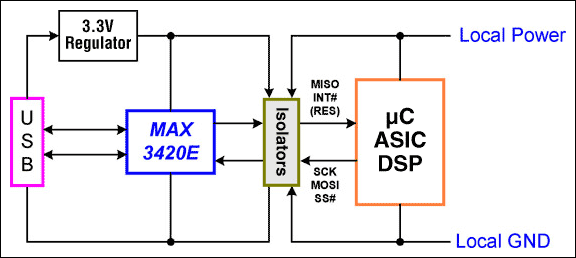
Figure 3. Isolating USB.
As shown in Figure 3 above, the SPI interface is an easy place to put optical isolation. This is because the SPI signals are unidirectional, and they can run at a low frequency to support low-cost optocouplers.
The SPI Interface
SPI is a simple serial interface that uses two data lines, a serial clock, and a chip-select signal. The SPI master drops SS# low to start a transfer, and then drives the serial clock, SCLK, to simultaneously clock data in and out of a slave device. The SPI master terminates a transfer by returning SS# high.
The SPI interface has four clocking modes, reflecting two mode signals called CPOL (clock polarity) and CPHA (clock phase). These signals are represented in the form (CPOL, CPHA). An interface expecting both positive edge SCKS and MOSI data to be available before the first positive clock edge, can operate in modes (0,0) and (1,1) without alteration. This property allows the MAX3420E to operate in either of these modes without requiring a mode pin.
Figures 4 and 5 illustrate identical data transfers between a microcontroller (the MAXQ2000, described later) and the MAX3420E. Figure 4 uses SPI mode (0,0) and Figure 5 uses SPI mode (1,1). The difference is the inactive level of the SCLK signal, low for mode (0,0) and high for mode (1,1).
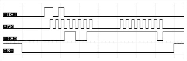
Figure 4. SPI interface operating in mode (0,0).
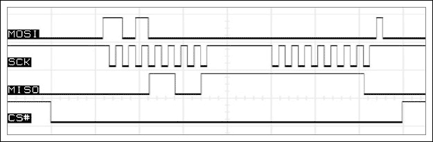
Figure 5. SPI interface operating in mode (1,1,).
The MAX3420E accepts a command byte as the first byte of every transfer. The command byte contains the register number and a direction bit. The second and subsequent bytes contain data. The eight bits, coming from the MAX3420E (MISO pin) while the command byte is being clock in (MOSI pin) in Figures 4 and 5, are USB status bits available every time that a command byte is clocked in. This feature is active only for interfaces that use the separate data pins, MISO and MOSI.
SPI Code
The key to writing general C code for the MAX3420E is to isolate the bare minimum of SPI operations in a separate module, and to customize only this module from SPI interface to SPI interface. At a minimum, this module needs to do only three things:
- Initialize_SPI
- Read byte
- Write byte
The example application here uses a hardware SPI unit. For applications that do not have such a unit, we will first review some generic C code for a bit-banged SPI interface.
Bit-Banged SPI
Init SPI
The Initialize_SPI function will change the most from processor to processor. It is responsible for assigning the particular I/O pins used by the interface, setting their directions, and then setting the initial conditions of SS = 1 and SCLK = 0. (We are making a mode (0,0) SPI master.)
Read Register, Write Register
rreg is a C function to read a MAX3420E register. The macros (all caps) insulate the function from various I/O schemes of various microcontrollers. Use of macros makes the code easy to read and processor independent. wreg is a routine to write a MAX3420E register.
If you change processors, you only need to change a handful of macros to use these routines. As an example, the macros below are for a microcontroller which does not contain a hardware SPI unit.
#define SCLK_HI OUTA = PINSA | 0x02;
#define SCLK_LO OUTA = PINSA & 0xFD;
#define SS_HI   OUTA = PINSA | 0x04;
#define SS_LO   OUTA = PINSA & 0xFB;
#define MOSI(v) OUTA = (PINSA & 0x7F) | (v & 0x80);
#define MISO inval |= PINSA & 0x01;

BYTE rreg(BYTE r)     // Read a register, return its value.
{
int j;
BYTE bv,inval;
inval = 0;
SS_LO
bv = r<<3;                                        // Left-shift the reg number, WRITE=0
for (j=0; j<8; j++)          // send the register number and direction bit
        {
        MOSI(bv)                             // put out a bit
        bv <<= 1;                      // shift one bit left
        SCLK_HI
        SCLK_LO
        }
for (j=0; j<7; j++)          // get 7 bits and shift left into 'inval'
        {
        SCLK_HI
        MISO
        inval <<= 1;                      // shift in one bit
        SCLK_LO
        }
SCLK_HI                            // one more bit, but don't shift 'inval' this time
MISO
SCLK_LO
SS_HI
return inval;                     // return the byte we read in
}

void wreg(BYTE r,BYTE v) // register, value
{
int j;
BYTE bv;
SS_LO
bv = (r<<3)+2;                    // Left-shift the reg number, set the WRITE direction bit
for (j=0; j<8; j++)  // send the register number and direction bit
        {
        MOSI(bv)                                // put out a bit
        bv <<= 1;                         // shift one bit left
        SCLK_HI
        SCLK_LO
        }
for (j=0; j<8; j++)  // send the register data
        {
        MOSI(v)                                 // put out a bit
        v <<= 1;                          // shift one bit left
        SCLK_HI
        SCLK_LO
        }
SS_HI
}
Hardware SPI
This section discusses the MAXQ2000 microcontroller mentioned earlier. In brief, the MAXQ2000 is the first of a family of low-power, 16-bit, high-performance RISC processors. The 'Q' in MAXQ2000 represents 'quiet,' indicating that the architecture is designed to coexist nicely with sensitive analog circuits. The MAXQ2000 has a built-in SPI port which makes it especially friendly to the MAX3420E . The following example uses the MAXQ2000 development kit and the MAX3420E to build a simple, but interesting Windows widget.
The MAXQ2000 hardware SPI unit provides SCLK, MOSI, and MISO, but not SS#. Because of variations in how SS# operates (for example, for accessing one byte vs. a burst of bytes), it is better to use a general-purpose I/O pin for SS#.
The MAXQ I/O Cell
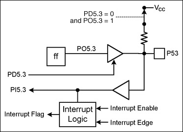
Figure 6. A MAXQ I/O cell.
Figure 6 shows the basic MAXQ I/O cell. The I/O port bits are labeled in the format 'port.bit' where 'p' is the port and 'b' is the bit. In this example we focus on I/O port 5, bit 3 (the pin is labeled P53).
Every I/O cell has a flip-flop which in this example is written using a bit called PO5.3. The 'O' represents output. You can always write this flip-flop; whether or not it gets connected to the pin depends on the direction bit. When configuring an output pin, in order to avoid glitches it is good practice to write the flip-flop before connecting it to the pin.
The direction of the P53 pin is set by a bit called PD5.3. The 'D' represents direction, and the D signal serves as the output enable for the pin driver: 1 = drive, 0 = float. The pin's state can always be read in a bit called PI5.3, where the 'I' represents input. Regardless of how the pin is driven, by the internal flip-flop (PD5.3 = 1) or by something external (PD5.3 = 0), the PI bit indicates the pin state.
There is a noteworthy feature in this structure. If the P53 pin is configured as an input (PD5.3 = 0), the output of the flip-flop is not used as an output and can, therefore, be reused as a pullup resistor switch. When D = 0, the O signal is redefined to mean, "connect a pullup resistor," as shown by the dotted line and switch in Figure 6.
Some I/O pins have interrupt capability, shown by the lower block in Figure 6. Interrupt blocks have three signals:
- A flag bit that is set when the interrupt request is active, and is reset by the CPU.
- An edge-select bit to determine whether a positive or negative signal transition causes the interrupt request.
- An interrupt-enable bit for the particular pin.
Our example application configures the MAX3420E INT output pin for a positive edge-triggered interrupt. On the MAXQ2000 side, the code directly tests the interrupt flip-flop for a pending USB interrupt, rather than using the MAXQ2000 interrupt system. The program does nothing but check the status of a pushbutton and respond to the USB requests, so a polling loop is all that is needed.
Init SPI
MAXQ2000 I/O pins are shared between general-purpose I/O and special-function hardware such as the SPI unit. To use special hardware, you first configure the hardware block, and then enable it to connect to the I/O pins. The SPI_Init() routine below sets pin directions, configures the SPI interface, and finally enables it.
void SPI_Init(void)
{
// MAXQ2000 SPI port
  CKCN = 0x00;              // system clock divisor is 1
  SS_HI                     // SS# high
  PD5 |= 0x070;             // Set SPI output pins (SS, SCLK, DOUT) as output.
  PD5 &= ~0x080;            // Set SPI input pin (DIN) as input.
  SPICK = 0x00;             // fastest SPI clock--div by 2
  SPICF = 0x00;             // mode(0,0), 8 bit data
  SPICN_bit.MSTM = 1;       // Set Q2000 as the master.
  SPICN_bit.SPIEN = 1;      // Enable SPI
// MAX3420E INT pin is tied to MAXQ2000 P60; make it an input
  PD6 &= ~0x01;             // PD6.0=0 (turn off output)
}
Read Register, Write Register
The functions below take advantage of the MAXQ2000's hardware SPI unit and, therefore, are smaller and faster than their bit-banged counterparts.
// Read a MAX3420E register, return its value.
BYTE rreg(BYTE reg)
{
BYTE dum;
  SS_LO
  SPIB = reg<<3;          // reg number w. dir=0 (IN)
  while(SPICN_bit.STBY);  // loop if data still being sent
  dum = SPIB;             // read and toss the input byte
  SPIB=0x00;              // data is don't care, we're clocking in MISO bits
  while(SPICN_bit.STBY);  // loop if data still being sent
  SS_HI
  return(SPIB);
}

// Write a MAX3420E register.
void wreg(BYTE reg, BYTE dat)
{
  SS_LO                   // Set SS# low
  SPIB = (reg<<3)+2;      // send reg. number w. DIR bit (b1) set to WRITE
  while(SPICN_bit.STBY);  // loop if data still being sent
  SPIB = dat;             // send the data
  while(SPICN_bit.STBY);  // loop if data still being sent
  SS_HI                   // set SS# high
}
Example: A Windows-Based Panic Button
This USB widget is a Windows-based USB HID (Human Interface Device), featuring a single 'panic' button. When you press the button, all active PC windows are minimized and you are looking at your desktop. Push it again, and all the application windows spring back to life.
USB keyboards are interesting. If you plug in several keyboards, they are all active simultaneously. Consequently, this panic button works in conjunction with your normal keyboard.
If the PC suspends, the panic button takes on a new role—it can serve as a remote wake-up button for the PC. This action is highly dependent on whether or not your PC supports wake-up from USB. Some PCS do, some do not. This button can help determine if your PC does have this capability.
This code example runs on the MAXQ2000 development kit with a small USB daughter board (containing the MAX3420E) plugged into an expansion connector.
USB Details
This application contains USB boilerplate code that does the basic work of enumeration. The personality for this device is completely described by the character arrays in the Panic_Button_Enum_Data.h listing at the end of this document.
This application uses two endpoints: the mandatory CONTROL endpoint zero, and EP3-IN, a single-buffered 64-byte endpoint. Although the MAX3420E contains two double-buffered 64-byte endpoints (EP1-OUT and EP2-IN), the throughput advantages of double buffering are not needed in this application.
A common HID misconception is that HID devices operate only at low speed. This application demonstrates that even something as slow as a keyboard can benefit from running at full speed. This is true because the keyboard uses less bus bandwidth, sending 12MHz instead of 1.5MHz packets.
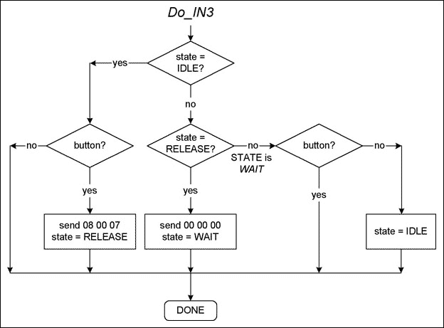
Figure 7. Flow diagram of the panic button.
Interrupt endpoints have a polling interval, which determines how often the USB host asks the IN endpoint for data. At every interval, we can expect the host to send an IN request to our device's endpoint 3. Figure 7 illustrates a simple state machine that handles these requests. Once the device is enumerated, the microcontroller repeatedly executes this routine. To simplify things, this application polls the interrupt pin for activity. If you have other operations running in the microcontroller, you will want to call the Do_IN3 function in response to an interrupt.
The state machine uses two global variables: state and button. C macros define three states: IDLE, RELEASE, and WAIT. The state variable is initialized to IDLE. The variable button is high if the pushbutton connected to the MAX3420E GPIN0 pin is pressed, and low otherwise. An endless loop in main() increments a button-check timer, and when expired, it reads the GPIO register in the MAX3420E to determine button state. This saves unnecessary SPI traffic.
While the button is up, the state diagram takes the two leftward branches and does nothing. If the button is pressed while in the IDLE state, it is time to send the keycode to clear the active windows. This is the sequence 08 (Windows key) 00 (reserved) and 07 (letter d). The next state is set to RELEASE, and the operation is done.
As soon as the MAX3420E dispatches this packet over USB, it generates another EP3-IN interrupt request indicating that the EP3-IN FIFO is again available for loading data. The Figure 7 function is entered again. This time state = RELEASE, so the function sends the sequence 00 00 00, indicating "keys up." The next state is set to WAIT, meaning, "wait for the button to be released."
Now the function only needs to use the WAIT-state branches to detect the button release. While the button stays down, nothing happens. When the button is released, the state diagram takes the two rightward branches and reinitializes the state variable to IDLE, readying the function for the next button press.
The code that executes most of the time is quite small. Here below is the entire function, which implements the flowchart in Figure 7:
void Do_IN3(void)
{
  switch(state)
  {
  case IDLE:
    if (button)
      {
                        wreg(rEP3INFIFO,0x08);  // "Windows" prefix key
                        wreg(rEP3INFIFO,0);
                        wreg(rEP3INFIFO,0x07);  // "D" key
                wreg(rEP3INBC,3);                       // arm it
                state = RELEASE;        // next state sends the "keys up" code
      }
      break;    // else do nothing (and the SIE will NAK)
//
  case RELEASE:
    {
                wreg(rEP3INFIFO,0x00);          // key up
                wreg(rEP3INFIFO,0x00);
                wreg(rEP3INFIFO,0x00);          // key up
        wreg(rEP3INBC,3);                               // arm it
        state = WAIT;                   // next state waits for the PB to be unpressed
    }
    break;
  case WAIT:
    if (!button)
      state = IDLE;
    break;
  default:  state = IDLE;
  } // end switch
}
Code Tidbits
A few details in the code deserve comment.
Time-Critical USB Events
The MAX3420E signals a remote wakeup by driving a 'K' state onto the bus for 10ms. To relieve the SPI master from the burden of counting off this time, the MAX3420E internally times this signal (and, in fact, every other USB time-sensitive event) and then gives the SPI master an interrupt when the interval is complete. The SPI master does not need to use its own timers for these events; it just starts the operation and then waits for the completion interrupt.
The ACKSTAT Bit
The functions rregAS and wregAS do one thing different from rreg and wreg; they set an ACK STATUS bit in the SPI command byte. The SPI master (the MAXQ2000, in our example) uses this bit to tell the MAX3420E that it has finished servicing the current CONTROL transfer, and therefore to terminate the CONTROL transfer by ACKing its status stage. Although ACKSTAT exists as an internal register bit, including it in the SPI command byte executes this frequently-used operation faster and with less code.
readbytes(), writebytes() Functions
The readbytes(), writebytes() functions take advantage of the MAX3420E's bursting capability. Instead of sending two SPI bytes per byte access (a command byte and a data byte), they first drop SS#, then send the command byte, clock in/out a burst of bytes, and finally raise SS# to terminate the SPI transfer.
Where to Find the Product ID
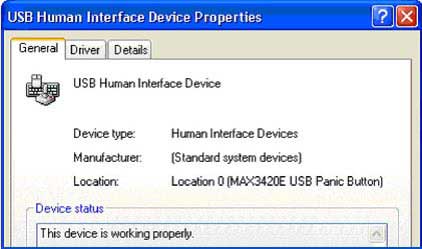
Figure 8. The Product ID string appears here.
The Product ID (PID) string (in Panic_Button_Enum_Data.h) appears as a short message the first time you plug in your panic button. This ID string pops up during the enumeration process that identifies the panic button as a HID, and associates it with the built-in Windows driver.
Every subsequent attachment is silent except for the little "ba-deep" Windows sound you hear when you plug in any USB device. If you want to check the device status anytime, go to the screen shown in Figure 8. You can reach this screen by right-clicking on My Computer, selecting Properties, the Hardware tab, the Device Manager button, expand the Human Interface Devices item, right-click on USB Human Interface Device, and select Properties.
USB Compliance
Perhaps you look at the code, and think, "This is a lot of work for a one-button USB device." This is true because there is a certain overhead associated with any USB device. Fortunately, USB is so carefully specified that this enumeration code can serve as a template (as in copy-paste) for any USB device.
Like all diligent developers, we want our designs to be certifiable by the USB-IF, which helps ensure that it will function without problems on any PC. This application passed the USB Command Verifier (USBCV version 1.2.1.0) and HID tests in the test suite available to developers on the USB-IF web site. Figure 9 below is the scorecard for this panic button.
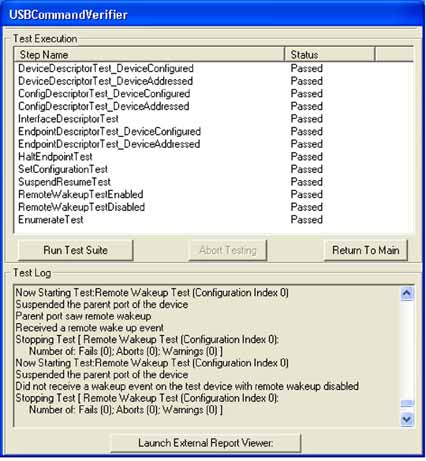
Figure 9. The test log and status report for the USB and HID tests on this panic button.
Conclusion
If you need to make a USB peripheral, consider using the MAX3420E. The device is small, easy to program, and comes with free example code. The MAX3420E adds I/O pins to your design, and plays nicely in any system that has SPI support. Because SPI is so easy to bit-bang, this design includes every microcontroller. If you want higher performance, you can clock the SPI interface as high as 26MHz.
A similar article appeared in the July 2005 issue of Circuit Cellar.
Appendix. Code listing
Related to this Article
Products
USB Peripheral Controller with SPI Interface
Low-Power LCD Microcontroller
Product Categories
Latest Media 21