Multiple LTC2315-12 ADCs Share SPI Bus
The data sheet doesn’t always show everything you need to know about using a part. For example, a common application when using multiple serial ADCs is to share the clock and data output lines to simplify the interface to the processor/FPGA. The data sheet for the LTC2315-12 12-bit 5Msps, SPI compatible ADC with an integrated bandgap and reference buffer does not show how to do this. Sharing these lines is possible as long as the ADCs are not converting simultaneously. The SDO output line of the LTC2315 becomes active when the CSL input goes low, starting a conversion. Therefore only one LTC2315 can be converting at any one time so that the SDO output lines do not fight with each other.
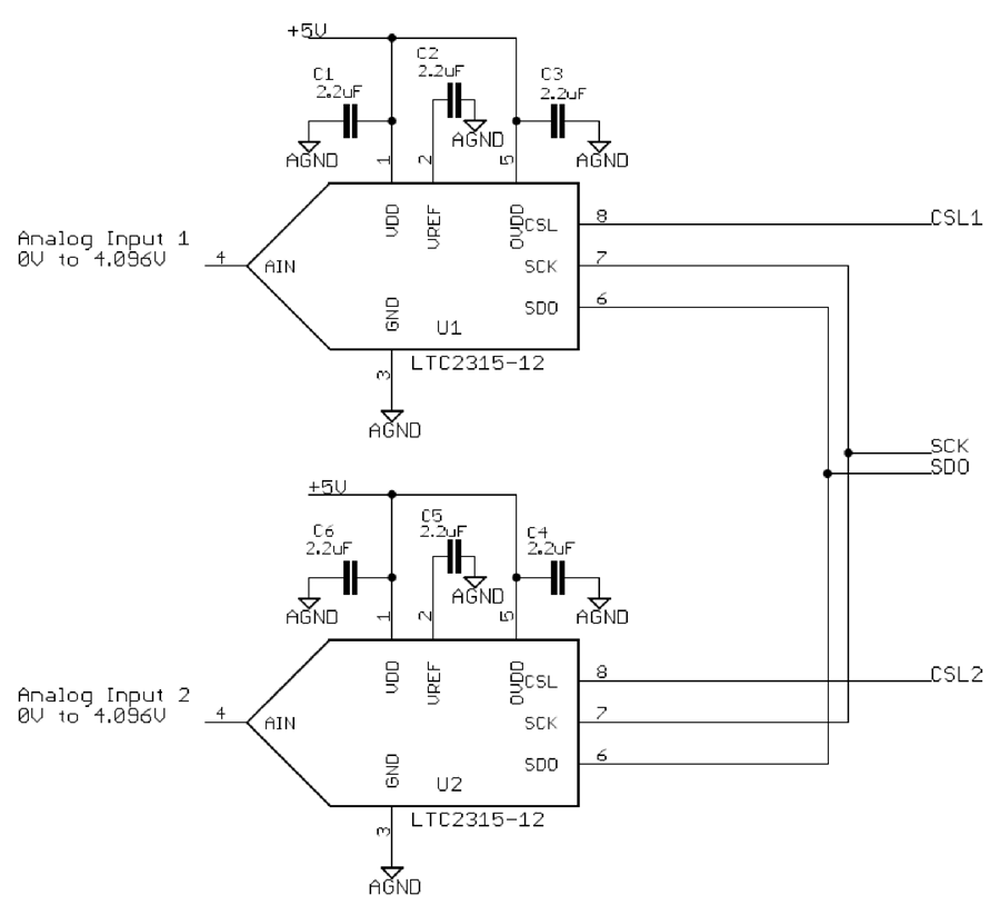

Figure 1. Two LTC2315-12s share a common SPI bus.
The circuit of Figure 1 shows two LTC2315s sharing a common SPI bus. The CSL1 and CSL2 input lines control which ADC is converting. Only one CSL line can go low at any time. Figure 2 shows a timing diagram for the two ADCs. Sufficient time should be allowed after the CSL1 line is brought back high before the CSL2 line is brought low so that the SDO output line of U1 returns to a Hi-Z state before the SDO output line of U2 becomes active. This same technique can be used for other ADCs in this family including the LTC2314, LTC2313 and LTC2312 12-bit and 14-bit ADCs, although the exact timing diagram will need to be adjusted to the specifications of the particular ADC.

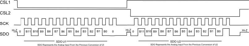
Figure 2. Timing Diagram shows two ADCs transferring data with shared SCK and SDO lines using the circuit of Figure 1.
关于作者
T他的职业生涯始于LTC,当时的职位是技术员,并向参与多个产品工作的Bob Dobkin、Bob Widlar、Carl Nelson和Tom Redfern学习,涉及产品包括运算放大器、比较器、开关稳压器和ADC。在此期间,他还花了大量时间来编写测试程序以对这些器件的特性进行表征。
关联至此文章
产品
资源
最新视频 21